Researchers at the University of Massachusetts Amherst have developed a laser-based technique to align 3D semiconductor chips, potentially overcoming long-standing challenges in chip manufacturing. The method uses concentric metalenses to generate holograms that reveal misalignments between chip layers at a smaller scale than ever before.
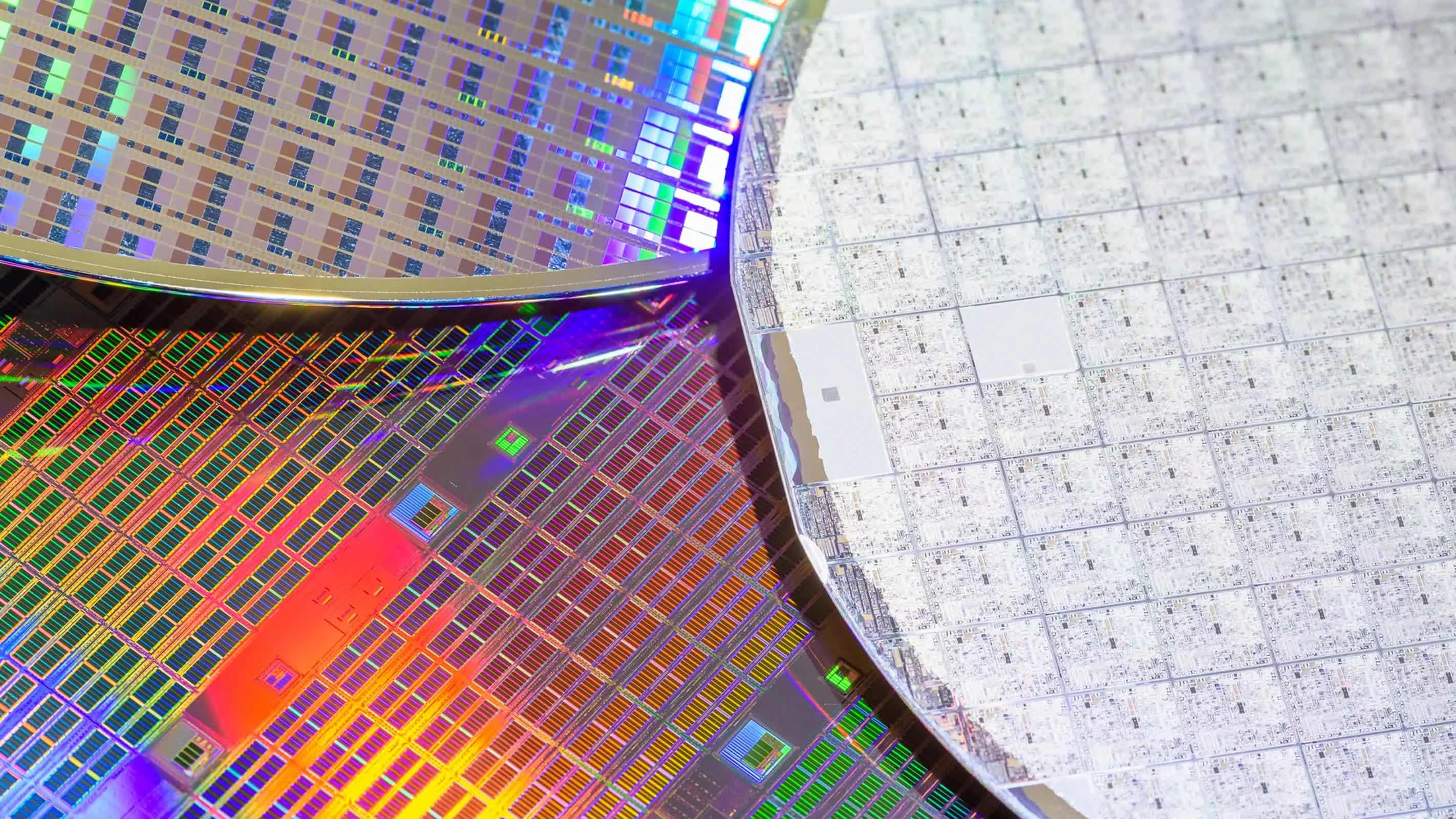
Traditionally, semiconductor chips are manufactured using two-dimensional processes. But as devices become more powerful and compact, the industry is increasingly turning to 3D chip design, which involves stacking multiple two-dimensional layers. This approach poses significant technical challenges—most notably, the need to align each layer with extremely high precision. Even slight misalignments can affect chip performance.
Amir Arbabi, associate professor of electrical and computer engineering at the University of Massachusetts Amherst and senior author of the study, said the traditional way to align two layers is to use a microscope to look at markings on the two layers, such as corners or crosshairs, and try to overlap them.
However, this microscope-based process is limited by physical gaps between layers and the need for refocusing, which can actually cause further chip drift and misalignment. Because the interlayer gaps are as high as hundreds of microns, the microscope cannot clearly see both crosshairs at the same time. Maryam Ghahremani, lead author of the study, explains that the movement required to refocus between layers can cause chip displacement. at the same time,Microscopy is also limited by the diffraction limit, which limits the smallest resolvable features to about 200 nanometers.
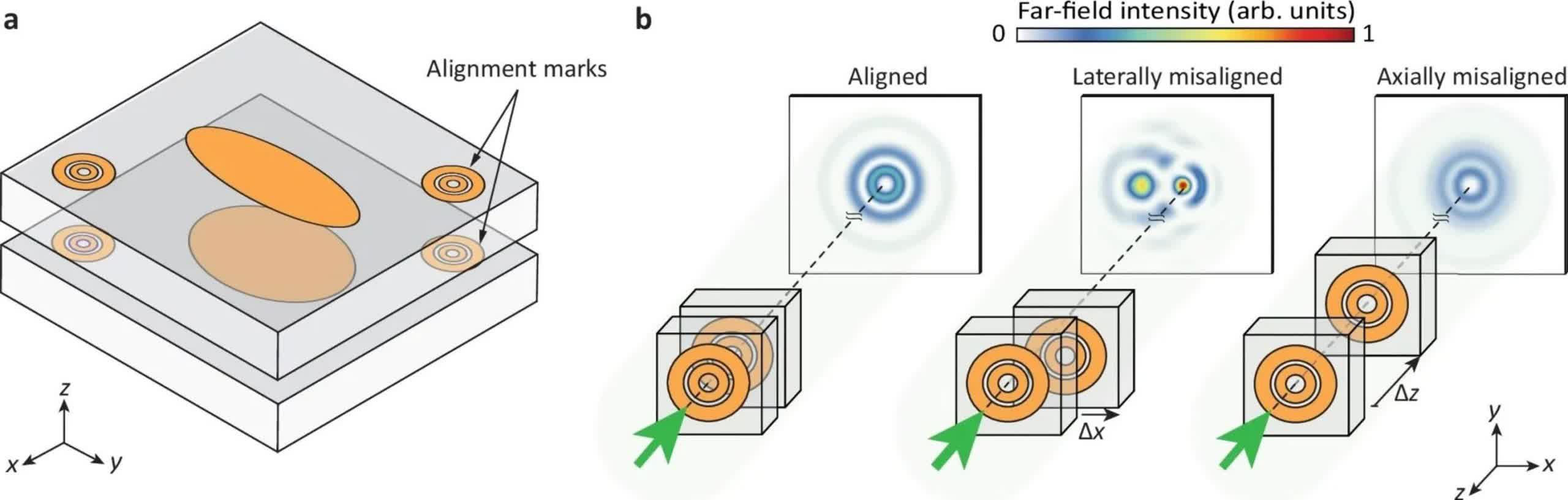
[Left] Semiconductor layers are stacked using concentric metalens as alignment marks. [Right] Light passes through these marks to project a hologram. The alignment and misalignment of the lenses determines the appearance of the hologram.
A new method developed at the University of Massachusetts Amherst circumvents these limitations. By embedding alignment marks made of concentric metalens on each chip and illuminating these marks with a laser, the researchers generated two interference holograms. The resulting interference pattern provides a direct visual clue of the chip's alignment, including the direction and magnitude of any misalignment.
"The interference image can show whether the chips are aligned, as well as the direction and extent of the misalignment," Ghahremani said.
The system's accuracy exceeded initial expectations. Although the team's initial goal was 100 nanometer accuracy, the method was able to detect misalignments as small as 0.017 nanometers in the horizontal axis and as small as 0.134 nanometers in the vertical axis. "Suppose there are two objects. By looking at the light passing through them, we can see whether one of the objects has moved an atomic-sized distance relative to the other," Albaby said.
This level of accuracy could have a significant impact on the semiconductor industry, where alignment errors have been an ongoing and costly challenge. Lowering the technical and financial barriers to ultra-precision chip alignment could make advanced manufacturing technologies more accessible to small businesses and startups.
The researchers also say the technology could be applied to compact, low-cost sensors. "Many physical quantities that you want to detect can be converted into displacements with just a simple laser and a camera," Arbabi said. Applications for this technology may include pressure sensors, vibration detectors, and other devices that monitor motion or environmental changes.