Intel originally planned to vigorously develop external foundry on the 18A process node, but the progress was very pessimistic and had to change to internal use and develop 14A foundry. After finally ushering in quarterly profit,Intel also briefly disclosed good news: "Initial feedback from external customers on 14A is encouraging!"
Of course, it is impossible for Intel to proactively announce which foundry customers it has, so it can only continue to wait patiently.
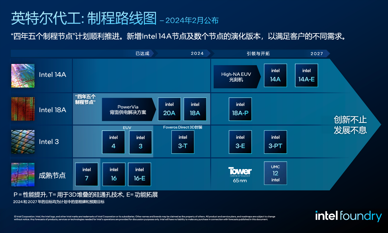
The Intel 14A process was announced early last year.It is said to be equivalent to 1.4nm and is expected to be mass-produced around 2027. Functionally expanded versions 14A-E will also be developed.
It is worth mentioning that 14A is different from any previous process.It was developed jointly with external partners from the beginning and is directly optimized for HPC, AI, mobile and other applications. It is expected to increase energy efficiency by 15-20% and reduce power consumption by 25-35%.
14A will use a new and expensive High NA EUV lithography machine for the first time in the industry, with a price of nearly US$400 million, 1.5-2 times the current price.
Intel has taken the lead in winning the world's first one and is testing it in its Oregon factory.
According to the plan, Intel will launch a new process node every two years in the future, and launch evolved versions of each node along the way.
Intel's foundry business also plans to achieve breakeven in 2027.