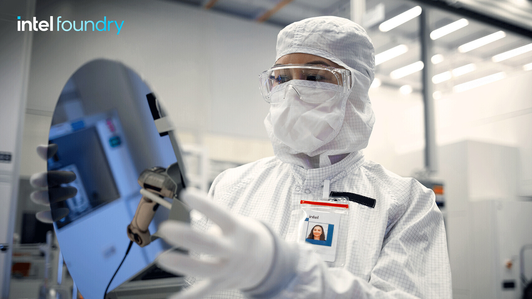
As a key part of Intel's foundry business, Intel's ongoing 14A process node is currently being jointly developed with a number of potential customers, with the goal of mass production in 2027. During this process, customers have the opportunity to participate in process design evaluation in advance to determine whether the node meets their future product needs in terms of performance, energy efficiency, and cost.
Patrick Moorhead, founder of the industry analysis agency Moor Insights & Strategy, said that the two Intel customers he has contacted who have an in-depth understanding of the 14A node are "very satisfied" with the current progress of the process. He believes that this node is expected to show strong competitiveness in the data center, PC and even the mobile chip market. This also means that Intel is trying to launch a new impact in the mobile field. He also pointed out that the industry generally expects Intel to launch version 0.5 PDK (Process Design Kit) of 14A as soon as possible so that more customers can obtain more specific technical parameters and design rules in the design stage; but even when the PDK is not yet fully ready, the feedback around 14A has been quite positive, forming a continuity with the previous advancement rhythm of the 18A node. Each new generation of process is iteratively optimized based on the mature experience of the previous generation.
On the manufacturing technology path, Intel plans to fully adopt high numerical aperture (High-NA) EUV lithography at the 14A node, becoming one of the first large-scale wafer fabs in the industry to transition from low NA to High-NA EUV. According to data previously disclosed by Intel, the company has used High-NA related production lines to process more than 30,000 wafers in a single quarter. At the same time, the new process has significantly simplified the manufacturing process of some key layers, compressing the process steps of some layers from about 40 to less than 10, thereby shortening the production cycle and improving overall production efficiency.
For customers who plan to entrust a large number of high-value chips to new foundry partners, in addition to process performance itself, safety and production capacity guarantees are also core considerations. Moorhead pointed out that when he recently communicated with the CEOs of almost all potential "anchor customers" (large-scale long-term foundry customers), they all emphasized that a key prerequisite is to be sure that the allocation of wafer capacity will be "fair and predictable" and will not squeeze the production arrangements of other customers because of the needs of a single customer.
At the production capacity level, the ASML Twinscan EXE:5200B dual-station High-NA EUV exposure machine introduced by Intel is regarded as one of the infrastructure supporting the 14A node mass production capability. A single piece of equipment can process about 200 wafers per hour. Combined with Intel's advanced factory layout in the United States and other regions, industry analysts believe that this generation of production line is expected to provide sufficient production capacity for multiple large customers at the same time after planning is completed, thus alleviating external concerns about the initial yield rate and production capacity ramp-up of the new process.