In the past thirty years, the global storage industry has completed a brutal and complete change of power. In the 1980s and 1990s, Japanese companies almost monopolized the DRAM market; after entering the 21st century, this throne was taken away by Korean manufacturers, thus establishing a long-term dominance spanning technology, scale and capital. Today, HBM has become one of the rarest and most profitable core devices in the AI computing power system. Korean manufacturers are enjoying the dividends, while Japan is basically absent.
However, just when everyone thought that Japanese storage had "lain flat", a very ambitious local company was emerging.
Storage history rewritten by South Korea
Japan was once synonymous with DRAM.
In the 1980s, several Japanese storage companies together accounted for more than half of the global DRAM market. DRAM is almost equivalent to the business card of Japan's semiconductor industry. At that time, Japan was at the peak of its global manufacturing expansion. Automobiles, home appliances, precision instruments, machine tools, and consumer electronics are internationally competitive in almost all industrial product categories, and semiconductors are the link with the highest technology density and highest added value in this industrial system.
Let’s talk about how Japan became the dominant player in DRAM. From the 1970s to the 1980s, the Japanese government led a series of national joint semiconductor R&D programs through MITI (Ministry of International Trade and Industry): including the Very Large Scale Integrated Circuit (VLSI) national project, the sharing of basic process results among enterprises, and the collaborative advancement of large enterprises in conjunction with universities and research institutions. This system has spawned a number of companies that are extremely mature in technology, materials, equipment, and manufacturing management: companies such as NEC, Toshiba, Hitachi, and Fujitsu.
In the mid-to-late 1980s, Japanese manufacturers once occupied more than 50% of the global DRAM market.
The core features of the Japanese model can be summarized in three points:
First, process orientation. Japanese manufacturers place great emphasis on process details, device reliability and long-term yield stability, rather than simply pursuing the "minimum node".
Second, create discipline. We attach great importance to the yield curve climbing speed, equipment stability, and production line consistency.
Third, industrial collaboration. Materials, equipment, wafer manufacturing, packaging and testing form a highly cohesive domestic industrial chain.
At that stage, the competition in DRAM was essentially: who could achieve mass production yields faster and more stably. Japan has a natural advantage in this regard.
Why did Japan lose its DRAM throne?
The turning point came in the 1990s. During this period, Japan's economic bubble burst, companies entered a long-term balance sheet repair period, and capital expenditures tended to be conservative.
At the same time, the DRAM industry has undergone structural changes: the market has begun to undergo strong cyclical fluctuations, products have gradually become standardized and homogeneous, and price competition has become increasingly fierce.
DRAM has gradually transformed from a technology premium product to an asset-heavy industry with high capital expenditures, high cyclical fluctuations, and low gross profit tolerance. This is extremely detrimental to Japanese companies, because Japanese companies generally pursue stable returns and find it difficult to accept long-term losses in exchange for scale. They prefer "profitable manufacturing" rather than "strategic loss expansion."
Coupled with the trade restrictions imposed by the United States on Japanese semiconductors, Japanese manufacturers are under additional pressure on exports to the United States, further weakening their ability to expand. As a result, Japanese manufacturers gradually withdrew from the main DRAM battlefield in the 1990s and shifted their resources to logic chips, MCUs, power devices, sensors and other fields.
South Korea's overtaking from behind relies on another set of logic: represented by Samsung, the South Korean government and chaebol groups have formed a highly bound industrial promotion mechanism. First, at the national level, semiconductors have been regarded as a strategic industry for a long time, providing low-interest loans, tax incentives, and land support; at the corporate level, they can also accept long-term loss cycles, trade aggressive capital investment for scale, and prioritize market share instead of profit.
After the Asian financial crisis in 1997, this strategy was further strengthened. Samsung counter-cyclically expands DRAM production and eliminates competitors through price wars. In the end, almost all Japanese manufacturers withdrew from the mainstream DRAM market.
Subsequently, SK hynix (pre-modern semiconductor) emerged in the mid-2010s, and the global DRAM market has become dominated by Samsung and SK Hynix, with the remaining manufacturers only retaining marginal shares.
After entering the AI era, this advantage has been further amplified. High-performance computing puts forward three core requirements for memory: extremely high bandwidth, extremely low latency, and extremely high capacity.
HBM (High Bandwidth Memory) has become a key device under this demand. The characteristics of HBM are: multi-layer DRAM die stacking, close packaging with GPU/AI accelerator, and the single value is significantly higher than ordinary DRAM. For Korean manufacturers that have already accumulated deep experience in DRAM stacking, packaging, and yield control, this is a natural extension of their advantages.
Therefore, Korean manufacturers quickly occupied HBM's dominant position, and high-end GPUs were almost inseparable from its supply. Naturally, they benefited from AI dividends, and the industry's voice was further concentrated.
The problem in Japan is that it has neither mainstream DRAM production capacity nor HBM technology accumulation, nor the ability to invest large-scale capital. In the current HBM industry chain, Japan's presence is almost only reflected in materials, equipment parts, and some packaging processes, but at the "product level", it is almost absent.
For Japan, the real concern may not be how much money South Korea makes, but whether Japan will completely lose the right to define "core device form" in the new round of computing paradigm changes.
Japanese storage strikes back
Against this background, a memory company named SAIMEMORY surfaced in early February 2026. SAIMEMORY was established in December 2024 and began operations in June 2025. It is a subsidiary of SoftBank, but has maintained a low profile before. It will not be until February 2026 that it will be publicly unveiled for the first time at the Intel Connection Japan 2026 event held by Intel.
On February 3, 2026, SoftBank announced that its wholly-owned subsidiary SAIMEMORY signed a cooperation agreement with Intel on February 2, 2026 to promote the commercialization of Z-Angle Memory (ZAM).
The name ZAM comes from the Z axis, which means that the chips are stacked axially in the vertical direction rather than just in the plane. Its theoretical advantages include: shorter data paths, more uniform thermal diffusion paths, higher scalable layers, and lower power consumption per unit bandwidth. In essence, this is an attempt to evolve from 2.5D stacking to a true 3D structure memory.
The essence of the structure of the current mainstream high-bandwidth memory is that Dies are stacked in the plane direction and interconnected through TSV and other methods. However, due to power and heat dissipation limitations, the current 16 layers of this structure are close to its limit, and the maximum number of layers is expected to be around 20 layers.
Intel is not simply a "strategic investor" in this project. Its key contributions come from: Next-Gen DRAM Bonding (NGDB), the basis of the Advanced Memory Technology (AMT) project supported by the U.S. Department of Energy. Intel Academician and Government Technology CTO Joshua Freeman said: Traditional memory architecture cannot meet the needs of AI, and NGDB defines a completely new approach.
The company will leverage underlying technologies and expertise proven through Intel's completed Next Generation DRAM Bonding (NGDB) initiative as part of the Advanced Memory Technology (AMT) program administered by the U.S. Department of Energy and the National Nuclear Security Administration through Sandia National Laboratories, Lawrence Livermore National Laboratory and Los Alamos National Laboratory. SAIMEMORY plans to develop a prototype product in fiscal year 2027 (ending March 31, 2028) and strive to achieve commercialization in fiscal year 2029. To this end, it will continue to promote research on innovative storage architecture and manufacturing technology.
Let’s talk about SoftBank’s abacus. SoftBank is betting on a new memory route that may skip the HBM generation. SoftBank is preparing “own memory” for AI infrastructure. SoftBank is becoming an AI infrastructure capital operator. SoftBank has stated that it will invest approximately 3 billion yen before the prototype is completed in fiscal 2027. This is an option investment: if it succeeds, it will control the entrance to the next generation of memory; if it fails, the losses will be controllable.
In the field of storage, Japan has adopted a "curve to save the country" strategy, seeking architecture-level jumps through structural innovation to avoid frontal large-scale wars. From the perspective of market environment, the scarcity of memory has also given Japan a window period. Currently, AI data centers consume most of the memory. According to TrendForce data, about 70% of the memory produced globally in 2026 will be consumed by data centers. Samsung and SK hynix both warned that shortages could last until 2027. Moreover, the industry consensus is that the proportion of memory consumed by AI data centers is rising rapidly, and memory supply and demand will remain tight in the next few years. As long as ZAM can be significantly better than HBM in a certain dimension of power consumption/bandwidth/cost, even if it only occupies a niche market, there will be commercial survival space.
Japan is not just betting on memory
After experiencing DRAM being completely surpassed by South Korea and advanced logic processes being monopolized by TSMC and Samsung, the Japanese industry has actually formed a highly consistent consensus: Japan can no longer replicate the sweeping semiconductor hegemony of the 1980s and 1990s. Regardless of capital volume, industrial scale, or risk tolerance, it is difficult for Japan to hedge head-on with China and the United States.
As a result, Japan's semiconductor strategy in recent years has seen a clear shift: from pursuing "bigger and more comprehensive" to ensuring that it has a seat at several key technology nodes that determine its future direction.
The first, and most symbolic, is the appearance of Rapidus. Rapidus is not a foundry established according to traditional business logic, but more like a "national capability company" with a shareholder lineup spanning automobiles, electronics, communications, Internet and semiconductors. Specializing in 2nm advanced processes, Japan is not dreaming about defeating TSMC in advanced processes, but wants to avoid a situation in which Japan has no "technical foothold" of its own in the field of the most advanced logic chip manufacturing. Therefore, Rapidus's cooperation with IBM and its equipment binding with ASML are essentially exchanging national power for an "advanced process ticket."
Second, in the foundry field, Japan successfully introduced Taiwan Semiconductor Manufacturing Company (TSMC) to build JASM Factory 1 and 2 in Kumamoto through huge subsidies, and cooperated with Sony and Denso. The first factory (mature/mid-level process) has been opened, and the second factory will introduce the 6/7nm advanced process. Try to achieve localized manufacturing and ensure supply chain security. This will also better enable Japanese equipment and material manufacturers to match the top OEM processes on-site.
Third, in terms of advanced packaging, Japan is planning to enter the Chiplet era. Intel has formed a research group called "SATAS" with 14 major Japanese suppliers (such as Ibiden, Resonon, etc.) to jointly develop back-end packaging technology. Japan has monopoly advantages in subdivisions such as photoresist (JSR, Tokyo Onka), packaging substrates (Ibiden) and slicing equipment (DISCO). This is Japan's bargaining chip in the field of advanced packaging.
Fourth, in the direction of AI accelerators, Japanese companies are also very restrained. Few Japanese companies have openly declared that they want to build general-purpose GPUs to challenge NVIDIA. Japan has now formed an AI chip matrix composed of the transformation of established giants, top laboratory incubations, and start-ups in vertical fields.
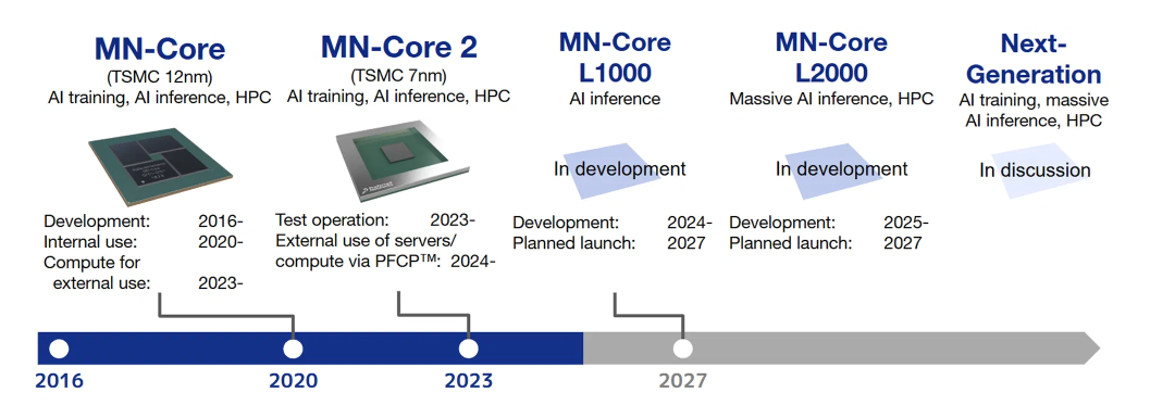
PFN is the most highly valued AI startup in Japan and the core force in Japan’s AI chip autonomy. The research and development of the first-generation MN-Core processor was launched in 2016, and two generations have been developed so far. In 2026, PFN has begun deploying its latest generation MN-Core L1000 and is working with companies such as SEGA to expand the capabilities of AI chips from high-performance computing (HPC) to a wider range of industrial and game rendering areas.
Source: PFN official website
MN-Core is a chip architecture tailor-made for matrix calculations in deep learning. During its design, it deliberately removed a large amount of complex control logic in general-purpose CPUs/GPUs. MN-Core's hardware architecture integrates a large number of dedicated matrix operation units (MAU) to efficiently perform core operations such as multiplication and addition. The entire architecture adopts the SIMD (single instruction, multiple data) idea: the same instruction drives a large amount of data in parallel calculations at the same time, and does not support complex conditional branches. On a higher-level structure, MN-Core organizes computing resources into "matrix operation blocks (MAB)". Each MAB consists of: 4 processor units (PE) and 1 matrix operation unit (MAU), and is combined using a hierarchical structure. Effectively, this architecture not only maintains a high degree of hardware specificity, but also retains a certain degree of programming flexibility through hierarchical and multi-mode support. It is very suitable for large-scale, regular matrix calculation tasks in neural networks.
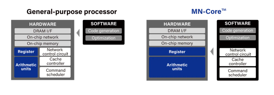
Comparison between MN-core and traditional general-purpose processor architecture (Source: PFN official website)
EdgeCortix is a dark horse in the edge AI field, headquartered in Tokyo and founded in July 2019. Its philosophy is to adopt a software-first approach and design an AI-specific processor architecture from scratch. Focusing on "edge-end" AI inference chips, its core product is the SAKURA-II series AI co-processor, which adopts an architecture called DNA (Dynamic Neural Accelerator). In January 2026, its SAKURA-II chip passed NASA's radiation resistance test and was verified for use on lunar missions and orbiting satellites. SAKURA-II supports billions of parameter models such as Llama 2, Stable Diffusion, DETR and ViT, with a typical power consumption of only 8W, meeting the needs of various edge-generated artificial intelligence applications in many application fields such as vision, language, and audio.
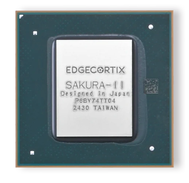
SAKURA-II chip (Source: EdgeCortix)
The laboratory of Japanese AI guru Professor Yutaka Matsuo has incubated a number of start-up companies. Although most of them are doing software, they are penetrating to the bottom through AI-SoC (system-on-chip). Companies such as EQUES are cooperating with semiconductor design factories to solidify specific visual recognition algorithms directly into chips.
The old Japanese chip giant is following the AI wave and achieving strategic transformation through "precise card positioning". Sony is leveraging its sensor advantages to develop visual AI chips; Renesas is stabilizing its automotive semiconductor footprint through in-vehicle AI MPUs; Fujitsu is relying on its supercomputer genes to continue to expand high-performance AI computing chips. They are trying to build new barriers in the niche vertical fields of AI.
Conclusion
Looking back, what Japan is doing is not so much "revenge" on South Korea as it is another bet on the fate of its own industry.
Japan no longer attempts to replicate the success of Samsung and SK hynix in terms of DRAM production capacity, and it no longer fantasizes about challenging NVIDIA head-on on the general GPU track. Instead, there is a calmer and more realistic route: in the advanced logic process, keep the starting point; in the advanced packaging, master the form; in the AI chip, enter the system; in the storage field, bet on architectural leaps.
The outcome of this gamble may not be known for many years. But at least Japan has returned to the poker table.