Samsung Electronics will later this month, after the Lunar New Year holiday (February 17 this year is the first day of the lunar calendar).Official batch delivery of HBM4 high-bandwidth memory chips to NVIDIA marks the first time that HBM4 chips have achieved large-scale mass production and shipment worldwide.
Industry sources show that Samsung Electronics has successfully passed all certification processes for NVIDIA HBM4 chips, and the delivery time accurately matches NVIDIA’s release plan for new generation artificial intelligence accelerators, including the Vera Rubin platform.
It is reported that NVIDIA plans to publicly display the Vera Rubin artificial intelligence computing platform equipped with Samsung HBM4 chip at the GTC 2026 conference held from March 16 to 19.
NVIDIA CEO Huang Renxun revealed at the CES 2026 exhibition last month that the Vera Rubin platform has fully entered the production stage. This also makes the market full of expectations for the official launch of the platform in the second half of 2026, and the timely delivery of Samsung HBM4 will lay a key foundation for its smooth implementation.
It is reported that the performance of the HBM4 chip produced by Samsung this time significantly exceeds the current industry standards. In terms of technology, the DRAM unit chip uses the 1c process (i.e., the sixth-generation 10nm-level DRAM technology), and the substrate chip uses the 4nm foundry process. This combination directly promotes the leap-forward improvement in HBM4 chip performance.
Specifically, the data processing speed of Samsung HBM4 can reach 11.7Gbps, which is about 37% higher than the 8Gbps set by the industry standard organization JEDEC, and is also 22% higher than the 9.6Gbps of the previous generation HBM3E; the single-stack storage bandwidth reaches 3TB/s, which is 2.4 times that of the previous generation.
The chip can provide 36GB capacity when using 12-layer stacking technology. After upgrading to 16-layer stacking in the future, the capacity can be further expanded to 48GB.
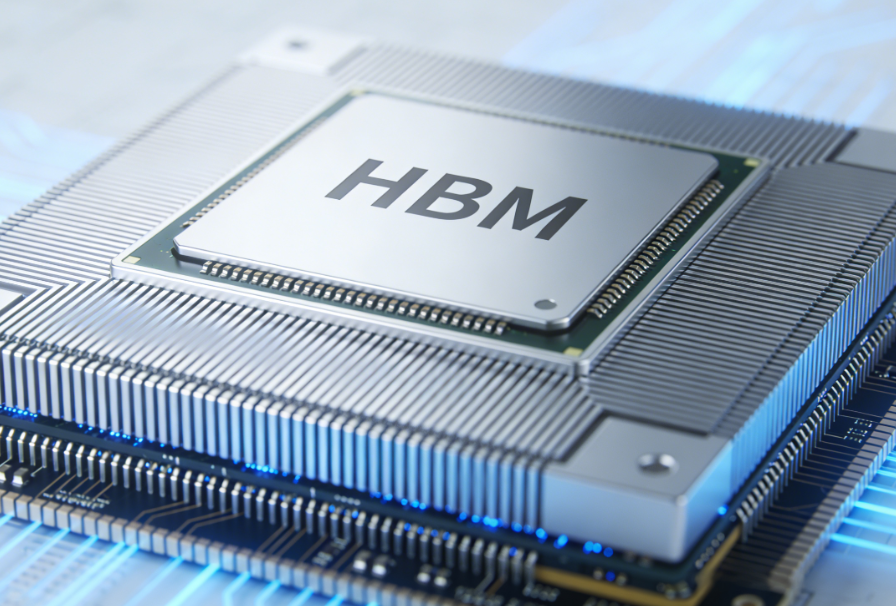
Simply put, HBM (High Bandwidth Memory) is a high-end memory chip designed specifically for AI accelerators and high-performance computing equipment. Its core function is to break the memory bandwidth bottleneck caused by increased computing power. It is also a core device in cutting-edge fields such as AI large model training and autonomous driving.
The current global demand for AI computing power continues to explode, and the HBM market demand is also growing rapidly. The large-scale mass production of HBM4 chips will not only promote the iterative upgrade of global storage technology, but also provide strong support for the performance breakthrough of the next generation AI computing platform.