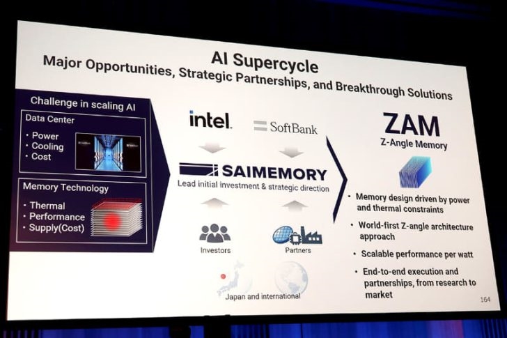
This is the first public display of Intel ZAM memory! Last week we reported that Intel would reach an in-depth cooperation with Saimemory, a subsidiary of SoftBank.Jointly developed a new next-generation memory technology called ZAM (Z-angle memory). Its maximum single-chip capacity can reach 512GB, and its power consumption is 40% to 50% lower than the current mainstream HBM memory. It is intended to break HBM's monopoly.
I thought it was still far away, but I didn't expect Intel to show its prototype products to the world so quickly. According to Japanese media PCWatch,At the Intel Connection Japan 2026 event, Intel publicly demonstrated its ZAM (Z-angle memory) memory technology prototype for the first time.
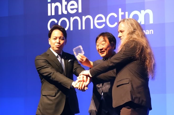
Joshua Fryman, Intel Academician and Chief Technology Officer for Government Technology, and Makoto Onho, CEO of Intel Japan, attended the event.
This event mainly focuses onHow ZAM helps existing solutions alleviate performance and thermal bottlenecks. This is also the first time that this technology has gone beyond research papers and press releases and been presented to the market in prototype form.
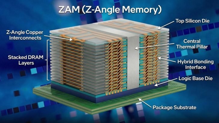
The core breakthrough of ZAM technology lies in the architectural design. It abandons the vertical wiring mode of traditional memory and uses a staggered interconnection topology to realize diagonal "Zigzag" wiring inside the chip stack. It uses copper-copper hybrid bonding technology to achieve efficient integration between chip layers.
At the same time, it combines capacitorless design with Intel’s mature EMIB interconnection technology.It not only achieves high-speed connection with the AI chip, but also significantly reduces the thermal resistance of the chip, making heat dissipation performance its core advantage.
Compared with the current mainstream HBM memory in the AI field, ZAM’s product advantages are very prominent:The maximum capacity of a single chip can reach 512GB, and the power consumption is 40%-50% lower than that of HBM. It can accurately solve the industry pain point of high energy consumption in AI data centers. The Z-shaped interconnection design further simplifies the manufacturing process and lays the foundation for subsequent large-scale mass production.
According to the information released at the event, Intel will be responsible for the initial investment and strategic decision-making in the ZAM project. The clear division of labor between the two parties makes the implementation path of this technology clearer.
In fact, Intel was an important player in the DRAM market in the early years. In 1985, it withdrew from the track due to competition from Japanese manufacturers.
Nowadays, global AI large model training and ultra-large-scale data center computing have driven the demand for computing power to rise exponentially. The bottleneck of the DRAM supply chain has become prominent. The monopoly of HBM memory has also brought about cost and production capacity issues, which provides an important opportunity for Intel's return. Relying on its profound technological accumulation in the fields of advanced packaging and chip stacking, Intel is trying to seize opportunities in the AI memory market with ZAM technology.
However, ZAM technology still faces a key test to achieve market breakthrough. Whether it can ultimately break the existing market structure depends on whether it can be adopted by leading companies in the AI industry such as NVIDIA, and whether it can successfully complete mass production and ecological construction in the future.