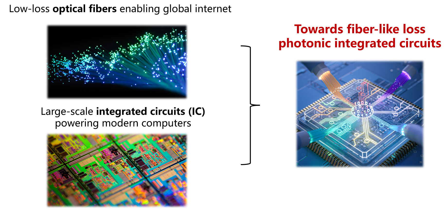
Researchers at the California Institute of Technology (Caltech) recently announced a major technological breakthrough. They have successfully developed a new technology that can achieve extremely low loss of optical signal transmission on silicon wafers, and its performance even approaches the level of traditional optical fibers in the visible light band.

This achievement marks a key step in the field of photonic integrated circuits (PICs), paving the way for the development of a new generation of optoelectronic devices with excellent coherence and extremely low energy loss. The research details a method of using optical fiber materials to build optical paths directly on the chip, and the related paper has been published in the journal Nature.
For a long time, optical fiber has become the cornerstone of global communication networks with its extremely high-purity glass material and atomically smooth surface, capable of transmitting massive amounts of data with extremely low loss. A team led by Kerry Vahala, a professor of applied physics and information science and technology at the California Institute of Technology, is committed to "transplanting" the manufacturing process of this optical fiber onto the silicon wafers used in computer chip production. The research team used the same germano-silicate glass material as optical fiber and used photolithography technology to build a light transmission channel called a "waveguide" on the chip. In order to solve the problem of surface roughness at the microscopic scale, the researchers innovatively introduced a process: putting the chip into a high-temperature furnace for "reflow" processing, so that the waveguide surface is melted and smoothed to the atomic level. This processing greatly suppresses light scattering loss and solves the key bottleneck that has long restricted the development of photonic integrated circuits in the visible light band.
Test results show that the performance of this new chip in the near-infrared band is equivalent to the current leading silicon nitride technology, while in the visible light band, its performance has achieved a qualitative leap, with the loss reduced to one-twentieth of the silicon nitride record. This ultra-low loss property has a profound impact on device performance, for example, lasers built using this technology have optical coherence times that are more than 100 times longer than existing versions. Hao-Jing Chen, the first author of the research paper and a postdoctoral scholar at Caltech, pointed out that the expansion of the wavelength coverage of this platform will support many important atomic operations, making it possible to implement chip-scale atomic sensors, optical clocks and ion trap systems.
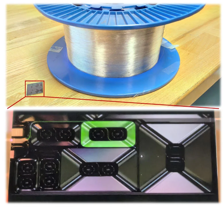
Although the size of these chips is only about 2 centimeters, their internal optical path design adopts a spiral structure, which greatly extends the propagation distance of light in a small space. Graduate student Kellan Colburn explained that for key optical components such as ring resonators, the longer the distance light circulates in them, the lower the losses and the better the performance of the device. Every 10-fold reduction in loss leads to a 100-fold improvement in coherence. This technology is not only as versatile as a "Swiss Army Knife" and can be widely used in fields ranging from high-precision timing, rotation measurement (gyroscope) to quantum computing and sensing, it is also of great significance in reducing the overall energy consumption of data center server infrastructure. Although the research team stated that the current results have not yet reached the ultimate goal, the significant progress in the past five years has drawn a clear blueprint for future photonic technology applications.