Taalas, a chip startup headquartered in Toronto, Canada, recently announced the completion of $169 million in new financing (total financing exceeds $219 million). At the same time, the company also officially announced that it would step out of stealth mode and begin to demonstrate its latest core technology.
The core technology of Taalas is to hard-code (etch) part of the structure of a large language model (LLM) (especially the weights and calculation logic) directly onto the silicon chip to make a highly customized chip, instead of loading the model into memory to run like a traditional GPU.
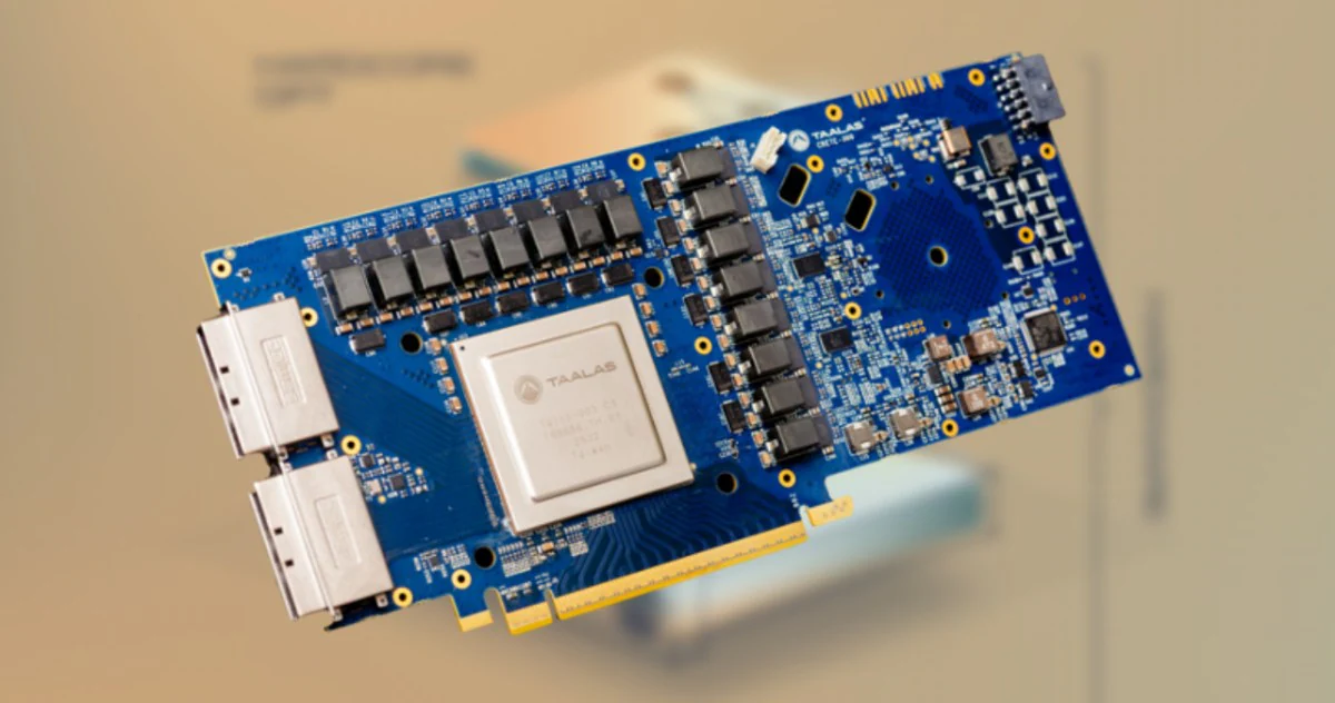
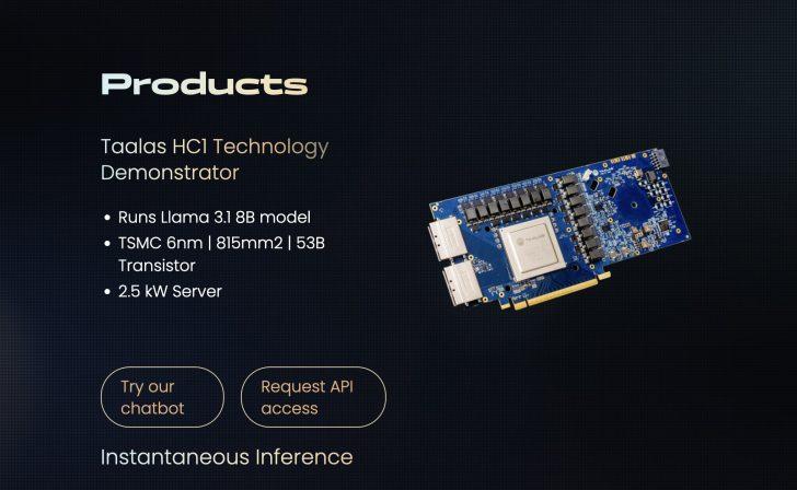
This hardware-level solidification approach turns large language models into "the chip itself is the model", so it can spit out characters at an extremely exaggerated speed when performing model calculations. For example, the single-user inference speed of the Taalas HC1 chip reaches 17,000+Tokens/second.
An easy-to-understand metaphor:
Traditional GPUs load the model into memory and then read and calculate it during runtime. In this case, the model is like a book placed on a bookshelf. Every time it is calculated, the chip has to repeatedly take the book out of the bookshelf, read it, calculate it, and write it back. The whole process is longer and consumes more power.
The H1C chip engraves the contents of the book directly onto the wall of the chip (implemented through transistors and fixed wiring). After the chip is powered on, the circuit itself grows into a model, and the data flow follows a fixed path without repeatedly reading the memory. It is equivalent to the chip itself being the model.
Speaking of which, this technology is actually very similar to the gate arrays of the 1990s. Taalas's innovation lies in using this ancient technology to approach the hard-wired complexity caused by LLM parameter sparsity and quantization.
The technical principle of chip-as-model:
Most of this hardware-level solidification approach is based on structured ASICs and custom masks. The core idea is to etch the weights and calculation structures of the model directly into the silicon chip using transistors and metal lines.
Taalas first made a nearly complete chip base (about 100 layers of metal/transistor structure). Most of the logic and storage have been completed, leaving only the last two layers of metal (mask) for final customization.
Changing these two layers of metal can write the weights of the specific model and part of the data flow path. This is like the pattern of the last two layers of copper foil on a printed circuit board that determines the specific functions. The cost and time are far lower than completely redesigning the chip.
The company designed a special structure that can store 4-bit weights + perform multiplication operations with very few transistors. The weights are not written in read-write memory, but hard-coded values like ROM read-only memory by using a mask to determine whether the transistor is conductive or not.
In actual calculations, there is no need to read weights, multipliers, and additions. Instead, the circuit itself completes the multiplication and addition operations, because the circuit connections and transistors have been configured according to the weights. The remaining small amount of flexibility relies on SRAM (high-speed static random access memory) to store the context cache.
Disadvantages of etching the model into the chip:
Computer majors should already know from the above technical principles that this technology also has fundamental disadvantages, that is, the model cannot be changed or upgraded after it is etched into the chip, that is, the chip can only use this model.
The first chip HC1 is etched with the Llama 3.1 8B version, which means that this chip can only use this model from the beginning of tape-out. However, the current AI industry is developing very fast and various new models are emerging in an endless stream. This approach of not being able to change and upgrade the model is the biggest disadvantage.
However, Taalas said that the entire process of customizing chips through a two-layer metal mask only takes about 2 months, which means that at least from a chip perspective, it is relatively easy to design new chips and run new models. This should help reduce costs, and customers may need to continue to purchase iterative chips according to their own needs.