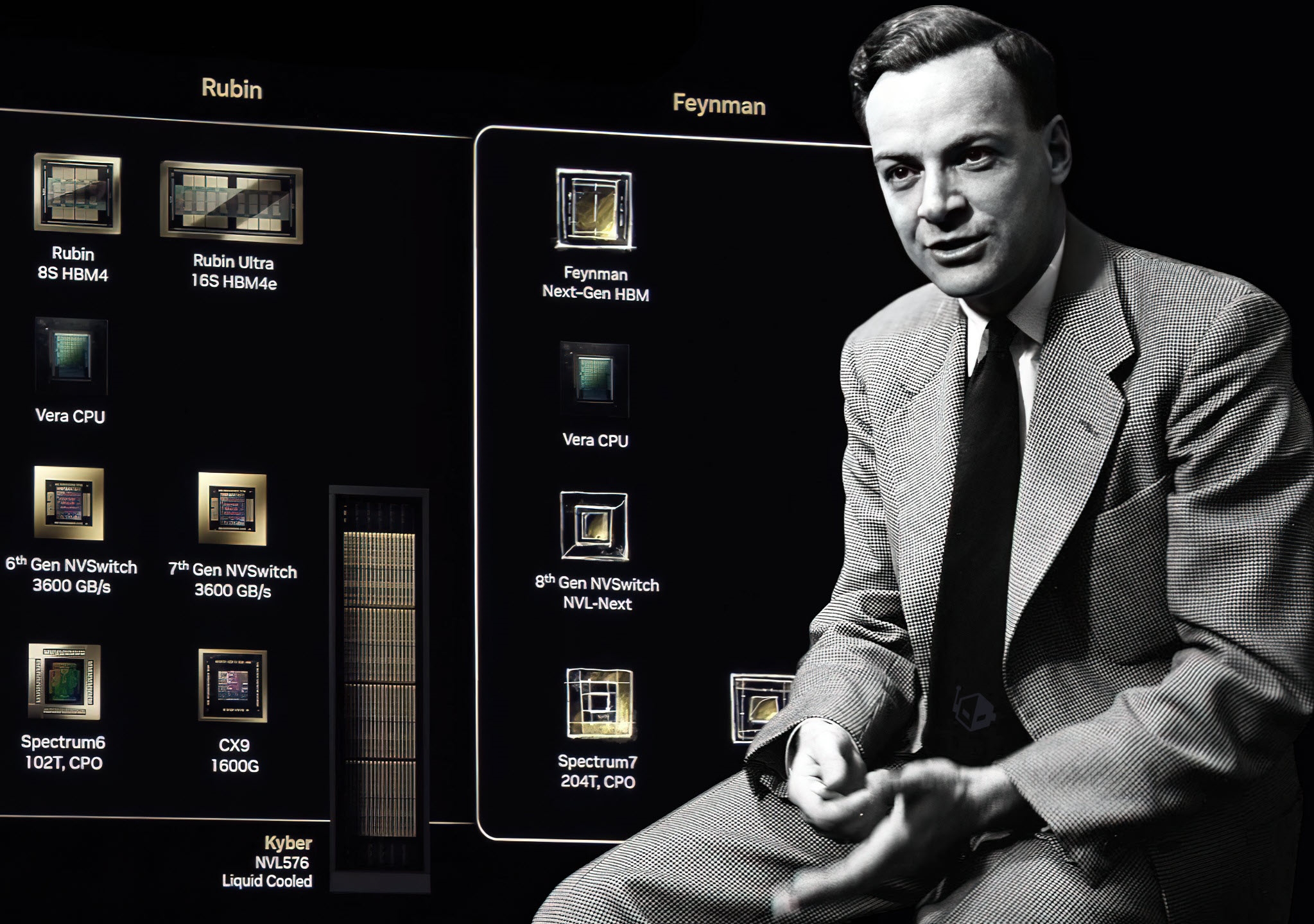
AttentionThe countdown has begun to the NVIDIA GTC 2026 conference, which is scheduled to open on March 15 in San Jose, California.According to the latest report and South Korean media "North Korea Business", NVIDIA's keynote speech will not only focus on Vera Rubin related technologies, butThe next-generation core product, the Feynman chip, will be unveiled for the first time, and will be equipped with the world's first 1.6nm process technology, becoming a milestone in the semiconductor field.
NVIDIA CEO Huang Jenxun previously revealed in an interview with Korean media:"We have prepared many new chips that the world has never seen before, which is not easy because all technologies are approaching physical limits."
He made it clear that this GTC 2026 conference will reveal “unprecedented” technology, the outside world generally believes that this is just a warm-up for the Feynman chip.
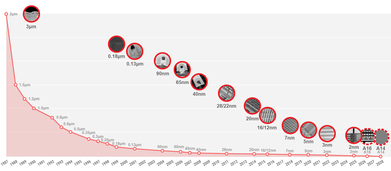
At present, the details of the Feynman chip have not been fully disclosed, but the confirmed core features are enough to shock the industry.The chip will be the world's first product to use TSMC's A16 (1.6nm) process, which is a major breakthrough in the semiconductor field. It has the world's smallest process node and also incorporates Super Power Rail (SPR) technology, which can improve performance while optimizing power consumption. NVIDIA is expected to become the first and only customer for initial mass production of TSMC's A16 process.
ps.PR moves the power supply lines to the back of the wafer to free up more signal line layout space on the front of the wafer to increase logic density and performance. SPR can also significantly reduce the voltage drop (IR Drop), thereby improving power supply efficiency.
In addition to its breakthrough process, Feynman's chip also has a major highlight: it will integrate the LPU (Language Processing Unit) hardware stack of Groq, an American smart chip company, for the first time. The current latency problem is a core pain point for GPU manufacturers, and integrating LPU units is the key to optimizing performance.
According to analysis, its LPU integration may adopt a hybrid bonding scheme similar to AMD's X3D processor, using LPU as an in-package integration option, but this will significantly increase the difficulty of chip design and production.
Industry predictions indicate that NVIDIA's display of the Feynman chip will most likely follow the format of the Vera Rubin chip launch that year, focusing on the chip's functions, architecture overview and mass production schedule.
It is reported that Feynman chips are expected to start mass production in 2028. According to NVIDIA's strategy, customer shipments may be postponed to 2029-2030.