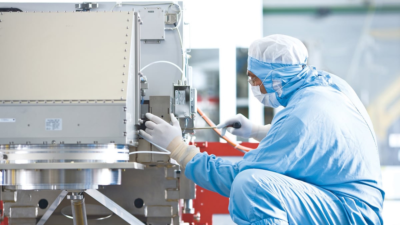
Dutch lithography giant ASML said its next-generation chip manufacturing equipment is ready and can be supplied to chip manufacturers for large-scale mass production, which is a major development for the chip industry. The Dutch company produces the world's only commercial extreme ultraviolet lithography (EUV) equipment, a critical piece of equipment that is indispensable for chipmakers.
According to data provided by ASML, the new equipment will help chipmakers such as TSMC and Intel produce more powerful and efficient chips because it eliminates some expensive and complex steps in the chip manufacturing process.
ASML Chief Technology Officer Marco Pieters said on Wednesday that the company planned to announce the data at a technology conference in San Jose on Thursday, marking an important milestone.
ASML has spent years developing these expensive next-generation devices, while chipmakers have been trying to determine under what circumstances it makes economic sense to use them for mass production.
But given that the current generation of EUV equipment is approaching the technical limit in making complex AI chips, the next generation of equipment, known as high numerical aperture EUV tools, will be critical to the AI industry, improving chatbots such as OpenAI’s ChatGPT and helping chipmakers complete their AI chip development roadmaps on time to meet surging demand.
The new devices will cost about $400 million, twice the cost of the original EUV devices.
ASML's data shows that high-numerical-aperture EUV equipment, which is now producing 500,000 dinner-plate-sized silicon wafers with significantly reduced downtime, is capable of drawing precise enough patterns to form circuits on chips, Peters said. Taken together, these three data points indicate that these devices are ready for manufacturers to use.
"I think we're at a critical point now where we need to look at the number of learning cycles that have been done," he said, referring to the number of tests customers have put the machines through.
Although the machines are technically mature, it will take two to three years for companies to conduct enough testing and development before integrating them into manufacturing.
"(Chipmakers) have all the necessary knowledge to validate these tools," Peters said.
Peters also said the equipment is currently operating at about 80% uptime, with plans to increase that to 90% by the end of the year. He noted that ASML plans to release imaging data that will be enough to convince customers to replace the multi-step processing of older generation equipment with a single-step high numerical aperture (High-NA) process. The equipment has processed 500,000 wafers, allowing the company to solve many technical problems.