In the artificial intelligence computing power competition, a long-undervalued link—chip advanced packaging—is rapidly evolving into a new bottleneck. Currently, almost all chips used for artificial intelligence computing must be packaged before they can be installed in hardware systems such as servers, cars, and robots to interact with the outside world. However, this key process is now highly concentrated in Asia, and the problem of tight production capacity has become increasingly prominent.
With TSMC planning to build two new advanced packaging plants in Arizona, and Elon Musk choosing Intel to provide packaging services for his custom chip project, this link in the industry chain that was previously regarded as a "back-end process" has come into the spotlight for the first time. John Vervey of the Center for Security and Emerging Technologies at Georgetown University pointed out that if companies do not significantly increase capital expenditures in advance, advanced packaging "will quickly evolve into a bottleneck" in response to the expansion of wafer fab production in the next few years.
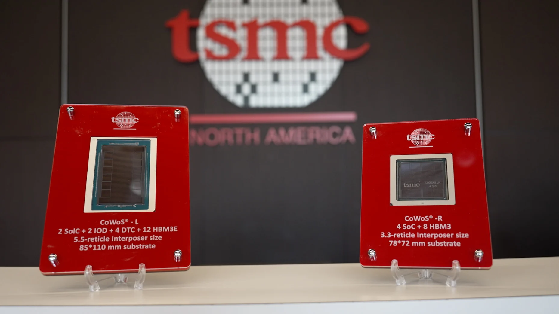
In a rare interview with CNBC, Paul Russo, head of TSMC's North American packaging solutions, said that business related to the company's most advanced packaging technology "is growing at a very impressive rate." Currently, TSMC's most advanced packaging process in mass production is "Chip on Wafer on Substrate" (CoWoS). Russo revealed that this business is expanding at a compound annual growth rate of about 80%.
In this field with the strongest demand, artificial intelligence giant Nvidia has booked most of TSMC's most advanced CoWoS production capacity, making it an absolutely heavyweight customer of Taiwan's leading foundry in advanced packaging. However, in terms of technical capabilities, US chip manufacturer Intel has been able to compete with TSMC.
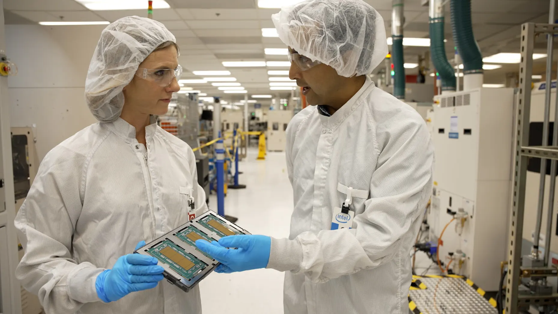
Intel has been committed to developing its foundry business in recent years, but it still lacks an "iconic major customer" in foundrying cutting-edge chips for external customers. In contrast, it already has a number of customers in the packaging business, including Amazon and Cisco, and has been providing advanced packaging services to external customers since 2022. On Tuesday, Musk further deepened his cooperation with Intel and announced that Intel would provide packaging services for the customized chips produced by SpaceX, xAI and Tesla in the planned "Terafab" factory in Texas. The factory aims to provide chips equivalent to 1 terawatt of computing power per year to support the development of AI.
Currently, most of Intel's final packaging processes are located in Vietnam, Malaysia and China, while factories in New Mexico, Oregon and Chandler, Arizona undertake part of its most advanced packaging processes. As the requirements for chip density, performance and energy efficiency in AI applications continue to increase, "Moore's Law", which traditionally relies on shrinking transistors to increase computing power, is approaching the physical limit. The industry has begun to regard advanced packaging as a key technology path to extend Moore's Law in the "third dimension".
In the past few decades, the industry usually cut a whole wafer into individual chips (die), packaged them separately, and connected them to terminal systems such as computers, mobile phones, and automobiles through substrates. As the complexity of artificial intelligence-driven chips has soared, more complex packaging methods have rapidly emerged in the past five or six years: multiple logic chips and high-bandwidth memory chips are no longer discretely packaged, but integrated into a larger system-level chip, such as a GPU. The core task of advanced packaging is to interconnect these different chips at high density within the same packaging system and ensure efficient communication between them and external systems.
Chip analyst Patrick Moorhead recalled that about five or six years ago, few manufacturers adopted such advanced packaging at scale. At that time, the packaging process was often regarded as an "after-the-fact process" and was even handed over to less experienced engineers. Now, he said, packaging is "clearly as important as the chip itself."
In the CoWoS segment that currently attracts the most market attention, Nvidia was revealed to have locked in most of TSMC's leading production capacity, so much so that TSMC had to outsource some relatively simple processes to third-party companies, including the world's largest chip packaging and testing foundries, ASE Semiconductor (ASE) and Amkor Technology (Amkor). ASE expects that its advanced packaging business revenue will double in 2026 and will build a large-scale new factory in Taiwan. Its subsidiary SPIL has also opened a new packaging base. NVIDIA CEO Huang Renxun personally attended the ribbon-cutting.
Faced with surging demand, TSMC is accelerating two new packaging plants in Taiwan and building two advanced packaging plants in Arizona, the United States. Currently, even the chips produced at TSMC's advanced wafer fab in Phoenix still need to be shipped back to Taiwan to be packaged before being shipped to customers, which means that the chips need to "travel back and forth" between the United States and Asia. TSMC has not yet made public disclosures on when its U.S. packaging plant will be put into operation.
Jane Vardaman, an authoritative researcher in the field of packaging at TechSearch International, said that locating packaging production capacity directly next to the Arizona wafer fab will significantly shorten the delivery cycle and avoid the transportation of chips back and forth between Asia and the United States, which will greatly improve customer satisfaction. Intel has also launched some packaging operations near its advanced 18A process chip manufacturing plant in Arizona to form an integrated layout of manufacturing and packaging.
Although Intel has not yet won an "iconic major customer" in 18A wafer foundry, Mark Gardner, head of its foundry services department, said that since 2022, the company has steadily provided packaging services to customers including Amazon and Cisco. On the other hand, Nvidia is also exploring the use of Intel's packaging capabilities, which echoes its previous investment of US$5 billion in Intel and the US government's US$8.9 billion investment in Intel in 2025. Moorehead believes that chip companies want to show the U.S. government that they are willing to cooperate with Intel, and that cooperation through packaging business is lower risk than directly handing over wafer manufacturing to Intel.
When asked whether Intel could eventually gain heavyweight customers in the chip manufacturing field through the "side door" of advanced packaging, Gardner said that for some customers, advanced packaging "does constitute an entry path." In his view, a "one-stop" service that integrates design, manufacturing and packaging in one place can bring many advantages.
Musk is expected to be one of the early customers to fully adopt Intel technology in both chip manufacturing and packaging. Intel released a statement on LinkedIn this week saying that the company has the ability to "design, manufacture and package ultra-high-performance chips" on a large scale and will help Musk's Terafab project achieve the ambitious goal of 1 terawatt of AI computing power production capacity per year.
On the technology evolution path, the industry is moving from traditional two-dimensional packaging to more complex 2.5D and even 3D packaging. For traditional chips such as CPUs, two-dimensional packaging is still the mainstream, but for highly complex computing chips such as GPUs, advanced packaging solutions such as TSMC's CoWoS have become key. Under the 2.5D architecture, chips are more closely interconnected through a layer of high-density connected "interposer", and high-bandwidth memory (HBM) can surround the computing chip, thus greatly alleviating the "memory wall" problem at the system level.
Russo explained that since it is difficult to stuff enough memory into a single computing chip to fully utilize its computing power, after TSMC launched CoWoS, it was able to attach HBM to the computing chip in a very efficient way and improve the overall performance from the architecture. Since TSMC took the lead in commercializing 2.5D CoWoS technology in 2012, it has gone through multiple generations of upgrades. TSMC stated that Nvidia’s latest generation Blackwell GPU is the first product to use its latest generation packaging technology CoWoS‑L, and it is this part of the most advanced production capacity that is now widely considered to be “almost wrapped up by Nvidia.”
As for Intel, its flagship advanced packaging technology is EMIB (Embedded Multi-die Interconnect Bridge). This solution is functionally similar to TSMC's interposer technology, but uses embedded silicon bridges instead of the entire interposer, and embeds small pieces of silicon wafers where high-density interconnection is required to reduce costs. Gardner said significant cost advantages can be achieved by "embedding very small pieces of silicon only where needed."
At the same time, companies such as TSMC and Intel are accelerating the layout of the next stage - true 3D packaging. Intel calls its 3D packaging technology Foveros Direct, while TSMC launches "System on Integrated Chips (SoIC)". Unlike 2.5D chips placed side by side, 3D packaging adopts a vertical stacking method to "stack" the chips. According to Russo, this allows multiple chips to "almost operate like a single chip" in terms of electrical characteristics and performance, bringing a new round of performance leaps.
Russo predicts that it will take a few more years before the market will see products packaged using TSMC's SoIC process being launched on a real scale. In this process, storage manufacturers such as Samsung, SK Hynix, and Micron are also promoting advanced packaging in their respective factories, using 3D packaging technology to vertically stack memory chips to build high-bandwidth memory products to meet the extreme demands for memory bandwidth and capacity for AI training and inference.
While accelerating the pace of shipments, storage and logic chip manufacturers are also promoting a new packaging process called "hybrid bonding", which uses copper pads to replace traditional solder bumps, significantly improving the density of chip stacking. Packaging expert Vardaman explained that by realizing direct connection of copper pads to copper pads, the distance between chips can be compressed to almost zero, which not only improves power consumption performance, but also brings better electrical characteristics, because "the shortest path is the best path."
In the AI era, the packaging link, which was once located at the back end of the supply chain and was inconspicuous, is becoming the new strategic commanding heights of the chip industry. On this increasingly competitive track, from Nvidia to Musk, from TSMC to Intel, all parties are vying for dominance in the "last mile" of the next generation of AI chips.