According to reports,Samsung Electronics has successfully produced a DRAM working wafer based on the 4F² architecture for the first time in the world, breaking through the physical shrinkage limit that traditional planar DRAM has long faced.It is reported that in February this year, Samsung publicly demonstrated this 16Gb DRAM prototype integrating 4F² architecture for the first time at the ISSCC 2026 conference.
Samsung completed wafer production using the 10a process in March and confirmed the normal operation of the wafer through characteristic testing. This achievement is the world's first practice of integrating 4F² cell structure and vertical channel transistor (VCT) process.
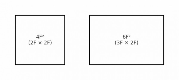
Technically, the 4F² architecture reduces the unit area of traditional DRAM from 6F² to a 2F×2F square structure, which can theoretically increase the capacity per unit area by 30% to 50% while taking into account the advantages of speed and power consumption.
To achieve this structure, Samsung introduced VCT technology to vertically erect the transistor channel and increase the channel length within the limited chip area, effectively alleviating the short channel effect and leakage problems encountered by traditional planar transistors during scaling.
On the other hand, Samsung uses inter-wafer hybrid copper bonding technology to manufacture memory cell arrays and peripheral circuits separately on different wafers and then stack them vertically to achieve ultra-high-density interconnection.
The channel material was also changed from traditional silicon to indium gallium zinc oxide (IGZO) to suppress leakage current in shrinking cells.
In the future, DRAM chips of the same size can be packed with more units. Terminal devices such as thin and light notebooks and smartphones are expected to achieve greater memory capacity and faster data throughput under the premise of small size and low power consumption.
Samsung has planned a clear roadmap for this—complete 10a DRAM development in 2026, conduct quality testing in 2027, and move into mass production in 2028.
SK Hynix plans to introduce 4F²+VCT at the 10b node, while Micron maintains the existing design route. Chinese manufacturers directly deploy 3D DRAM due to EUV restrictions.