Feminist Hacking released an open source project on the blog, uses natural clay to make a workable PCB printed circuit board. The entire process draws on prehistoric pottery technology, and the entire process from soil mining, shaping to firewood firing is completed by hand.
This project originated from the team’s reflection on conflict minerals in smart device hardware. They noticed that ceramic itself is an important material for electronic components such as capacitors, piezoelectric components and resistors, so they tried to use clay to replace traditional PCB substrates.
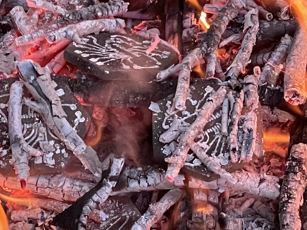
Different from commercial porcelain clay and high-temperature kilns, the team learned the prehistoric technique of open-air fire-firing clay from a pottery craftsman. After two days of practice, they mastered the process from local soil collection to firing into shape.
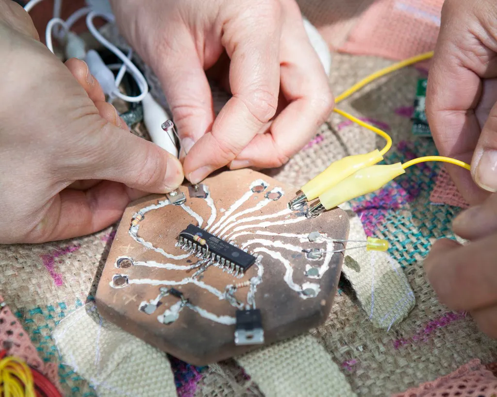
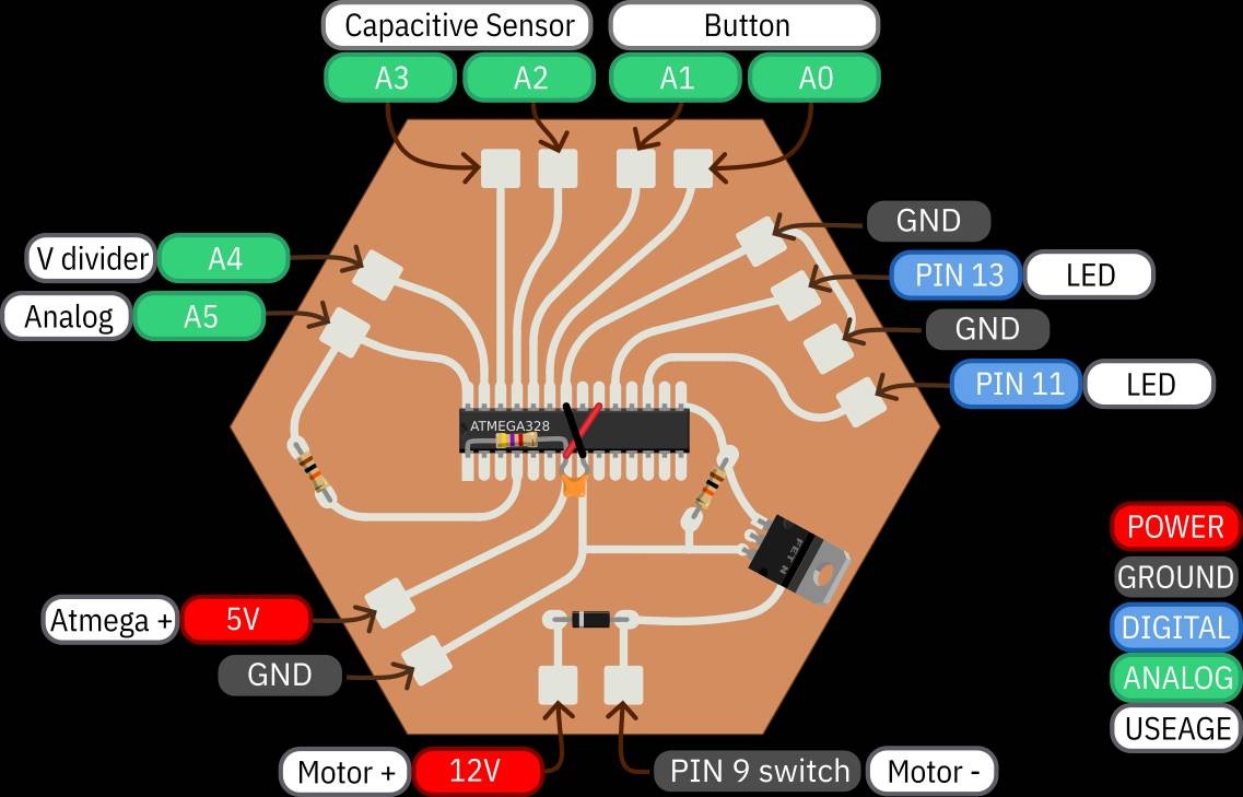
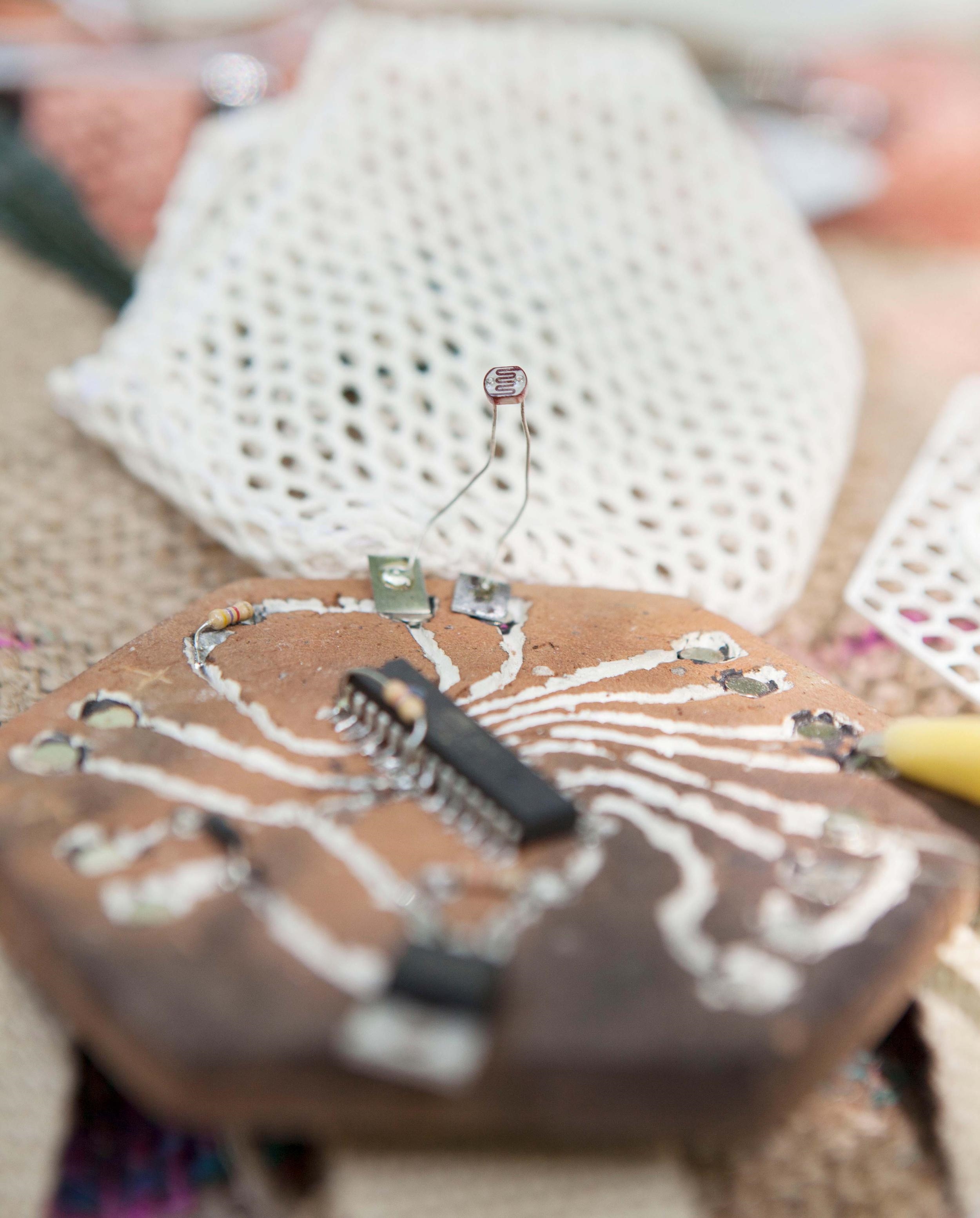
The production process is roughly divided into several steps: collecting and blending natural clay; After removing bubbles and impurities, press it into a clay sheet of about 10 × 10 cm; use a 3D printed mold to press out circuit trace grooves on the clay sheet, with a depth of about 1.5 mm; after drying naturally for one day, manually fill and coat the traces with silver-based conductive paint.

The silver paint chosen by the team is produced by a German company. The raw material comes from waste silver powder recycled by jewelers. The supply chain is traceable, and the coating is additionally thickened at the nodes that need to be welded.


TAG PH8The biggest technical challenge is the firing process. The clay will shrink by about 5% during the firing process. The team calibrated the mold size and groove depth after many trials and errors to ensure that the wiring accuracy of the finished product meets the welding requirements.
The project is fully open source, with a blog providing detailed production guides and PDF documents, and a GitHub page containing program code, welding instructions and 3D printing files.