Under the wave of computing power driven by generative artificial intelligence, TSMC, the world's leading wafer foundry, is advancing the layout of ultra-advanced processes at full speed. It plans to lay the foundation for the 1-nanometer era simultaneously before and after mass production of 2 nanometers, further widening the gap with Samsung in the field of high-end processes.
According to reports, the first batch of 2-nanometer chips is expected to be unveiled within this year, and most large customers will use TSMC's N2 and N2P process nodes, but this is only the starting point for competition in advanced processes. TSMC has begun planning a production route beyond the "ceiling" below 2 nanometers and initiated preliminary preparations for the 1 nanometer process, hoping to continue to consolidate its dominant position in the high-performance and energy-efficient chip manufacturing market in the next few years.
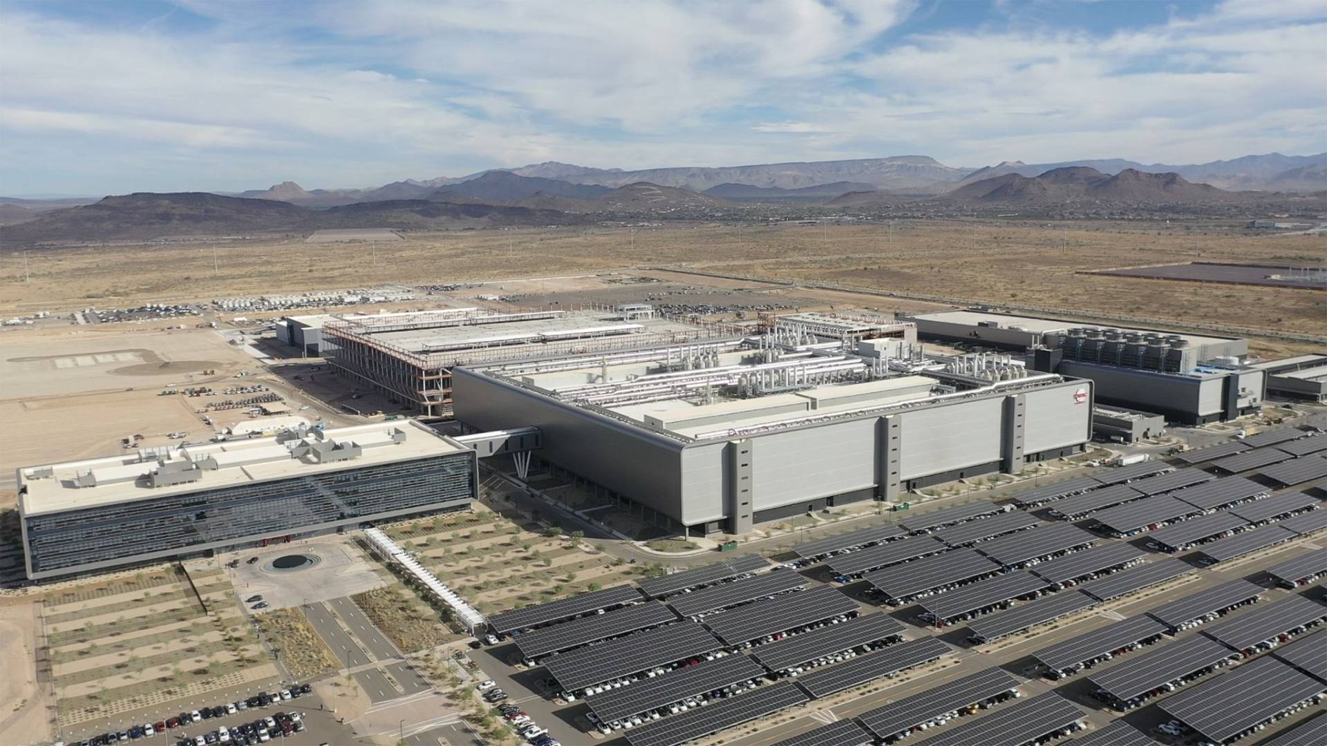
In order to meet the continued surge in order demand and take into account long-term production expansion plans, TSMC is currently building a number of new factories, including 1-nanometer-related production lines, with a total of 12 factories. These factories will become important production bases for 2-nanometer, A14 (approximately 1.4 nanometer) and subsequent more advanced nodes. Against the backdrop of rapidly growing demand for cutting-edge processes in areas such as artificial intelligence, data centers, high-end mobile phones and personal computers, TSMC is seen as one of the most well-prepared companies in this round of capital and technology competition.
However, it still takes time from site planning to formal mass production. According to reports, TSMC’s process of acquiring new factory land through the third phase of Longtan’s expansion plan is not expected to be officially launched until 2029, which means that large-scale mass production of the 1-nanometer process may not be realized until 2030 or 2031. Industry insiders pointed out that the research and development, verification and factory construction of advanced process nodes require long cycles and high investment. TSMC chose to deploy in advance not only to ensure production capacity, but also to seize the opportunity in the "race against time" with competitors.
In contrast, Samsung's pace in advanced process nodes is also accelerating, but the challenges it faces are more prominent. The report mentioned that Samsung plans to start mass production of 1-nanometer wafers in 2029, and has taken the lead in building a 2-nanometer process production plant in the United States, trying to improve its foundry competitiveness through geographical layout and technological breakthroughs. However, the key issue plaguing Samsung is not the speed of node advancement, but yield and process stability - which directly affects customers' confidence in its long-term cooperation.
Previous analysis pointed out that even if Samsung seizes the opportunity to introduce the 2nm process on a large scale before TSMC, its positioning among customer groups will still be closer to an "alternative solution" rather than a first-line preferred foundry that can compete head-on with TSMC. Only with significant improvements in yield and reliability can Samsung win more core orders in the high-end foundry market and truly shake up TSMC's current leading position.
In this context, Samsung is believed to stay on the 2nm node for a longer period of time in exchange for process maturity and yield improvement, hoping to expand its customer base and narrow the gap with TSMC in the high-end process war. However, judging from the current progress, TSMC has set its sights on launching 1-nanometer mass production around 2030. Once it proceeds as scheduled, it will continue to maintain a clear lead in the field of ultra-advanced manufacturing processes in the next few years.
Industry analysts believe that driven by AI inference and training chips, ultra-large-scale data centers, and high-end terminal equipment sensitive to energy efficiency, nodes of 1 nanometer and below will become the focus of capital and technology competition in the next stage. As TSMC and Samsung accelerate their respective layouts, competition in the high-end foundry market will become increasingly fierce. However, in the foreseeable future, TSMC will still have the upper hand on the road to 1nm by virtue of its process maturity, economies of scale and customer structure advantages.