SK Hynix demonstrated the next-generation HBM4E high-bandwidth memory sample at Computex 2026, focusing on the AI data center GPU platform to be launched by Nvidia, AMD and other manufacturers. As the scale of generative and inferential AI models continues to expand, the industry's demand for higher bandwidth, larger capacity, and more energy-efficient storage continues to rise. HBM4E is regarded as another major evolution based on HBM4.
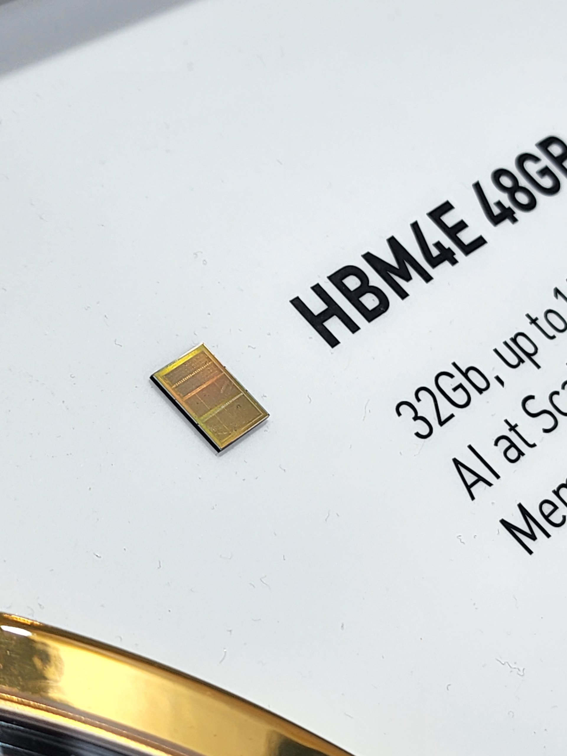
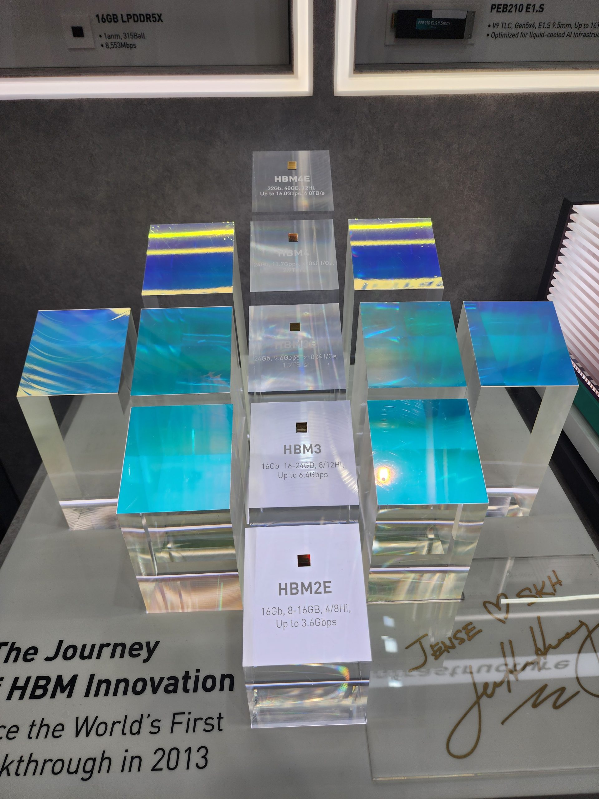
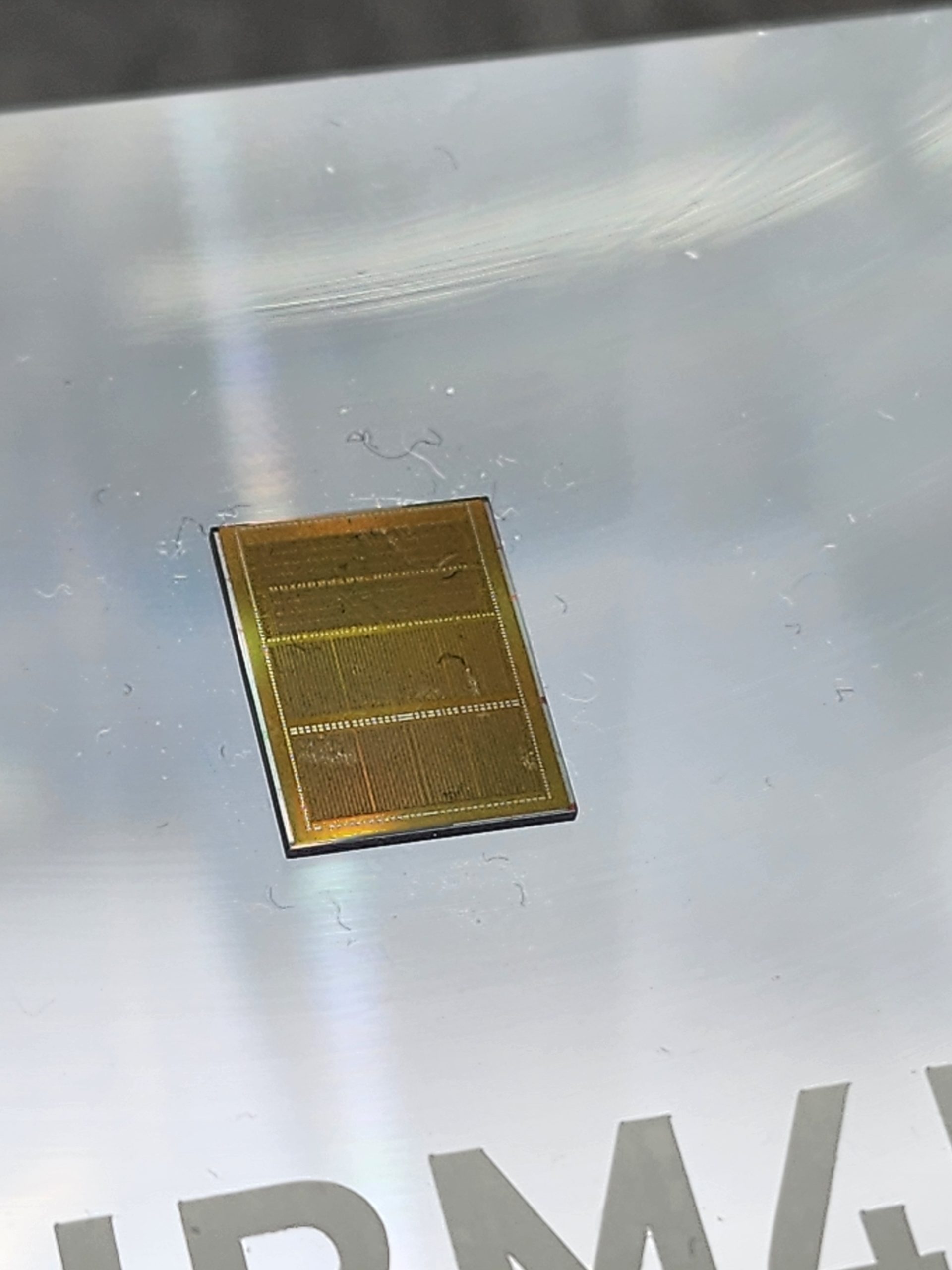
According to reports, the HBM4E single chip on display this time uses a 32Gb chip, which increases the die density by about 33% compared to HBM4. In terms of stacking structure, HBM4E can achieve 48GB capacity through 12-layer stacking. Previously, 16-layer stacking was usually required to achieve the same capacity. This means that while maintaining the same capacity, the packaging height and complexity are expected to be reduced, leaving more room for system design. In terms of performance, HBM4E's single-pin rate can reach up to 16Gbps, which is about 37% higher than HBM4, and its single-pin bandwidth can reach 4TB/s, setting a new bandwidth high for this type of product.
Industry insiders pointed out that new generation AI data center GPUs such as NVIDIA Rubin and AMD MI400 series will successively adopt HBM4 memory solutions this year, and HBM4E is regarded as the upgrade direction of subsequent products. SK hynix displayed HBM4E samples at the exhibition in advance, indicating its active layout in the next stage of HBM competition. The company predicts that HBM4E will first appear on the Nvidia Rubin Ultra GPU planned to be launched next year. Subsequent generations of products may use high-density packaging of multiple GPUs and HBM4E cores to further increase the upper limit of AI computing power and memory bandwidth.
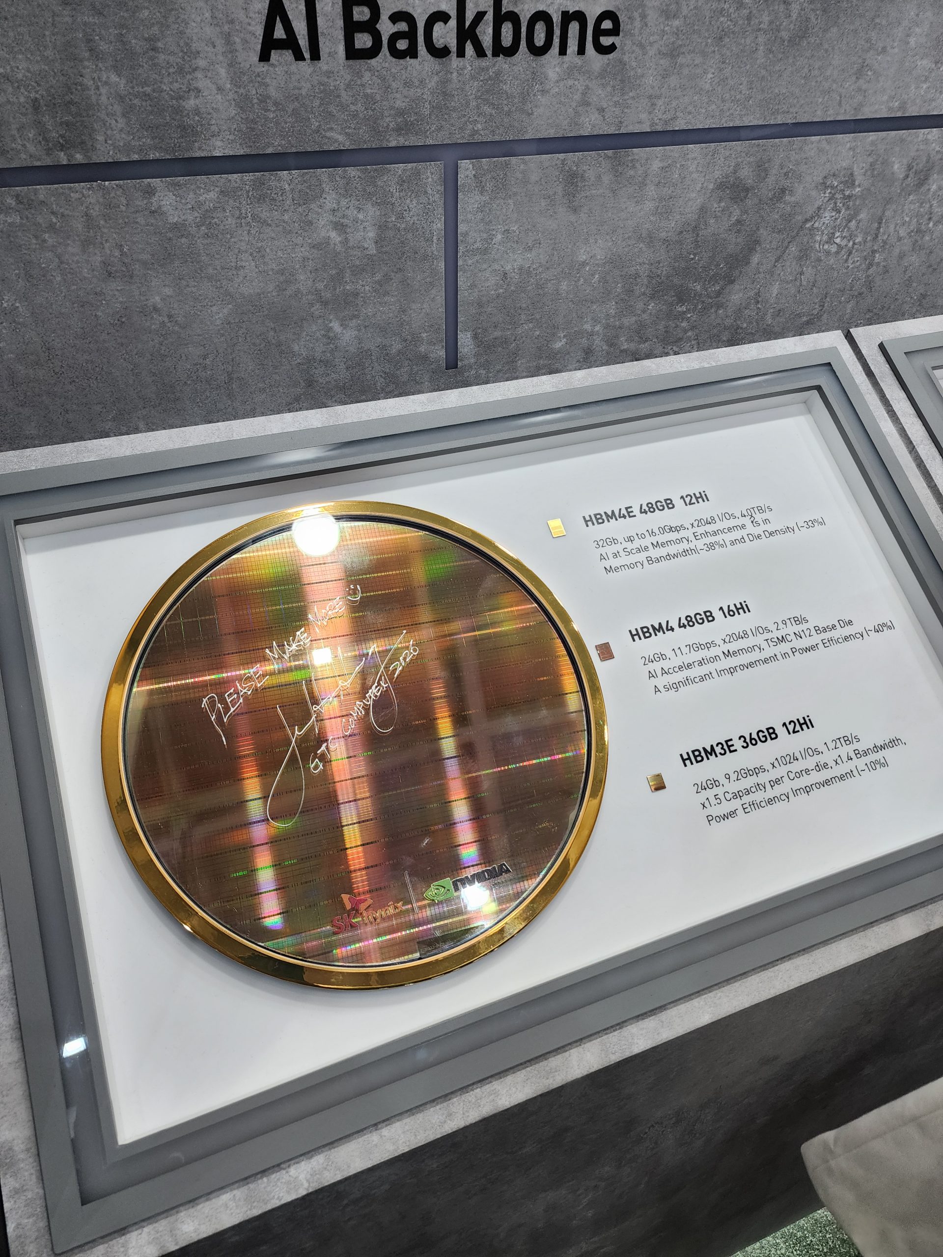
From the perspective of technology evolution path, HBM4E continues the iterative thinking of the HBM family in terms of bandwidth and energy efficiency. The previous HBM3E has achieved bandwidth and power consumption improvements of 1.2TB/s per chip in a 36GB, 12-layer stack configuration, while HBM4 has further improved the pin rate and overall bandwidth in a 48GB, 16-layer stack configuration. Currently announced parameters show that HBM4E achieves simultaneous improvements in bandwidth and power consumption efficiency through higher single-core density and 12-layer stacking design under the same 48GB capacity, helping to alleviate memory bottlenecks in high-load scenarios such as AI inference and training.
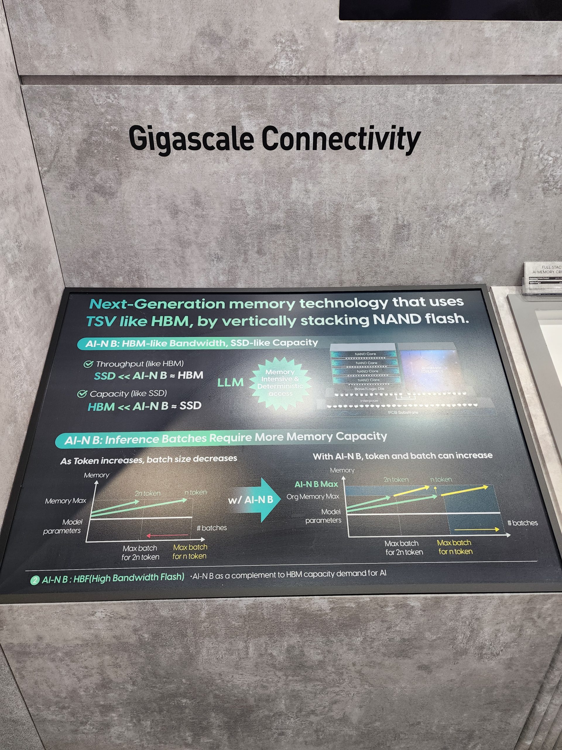
In addition to the HBM product line, SK Hynix also revealed its new stacked NAND solution "AI-N B" for the AI era during the same period of the exhibition. This solution draws on HBM’s through-hole silicon via (TSV) stacking idea to stack multi-layer NAND chips vertically to achieve the combined capabilities of “HBM-level bandwidth and SSD-level capacity.” The goal is to provide a higher-throughput storage system for large-scale AI inference while alleviating the industry pressure caused by the current tight supply of high-bandwidth storage. This idea has certain similarities with the technical paths such as HBF and Z-Angle proposed by other manufacturers in the industry. They are all trying to bridge the performance and cost gap between high-bandwidth memory and large-capacity storage through three-dimensional stacking and high-speed interconnection.
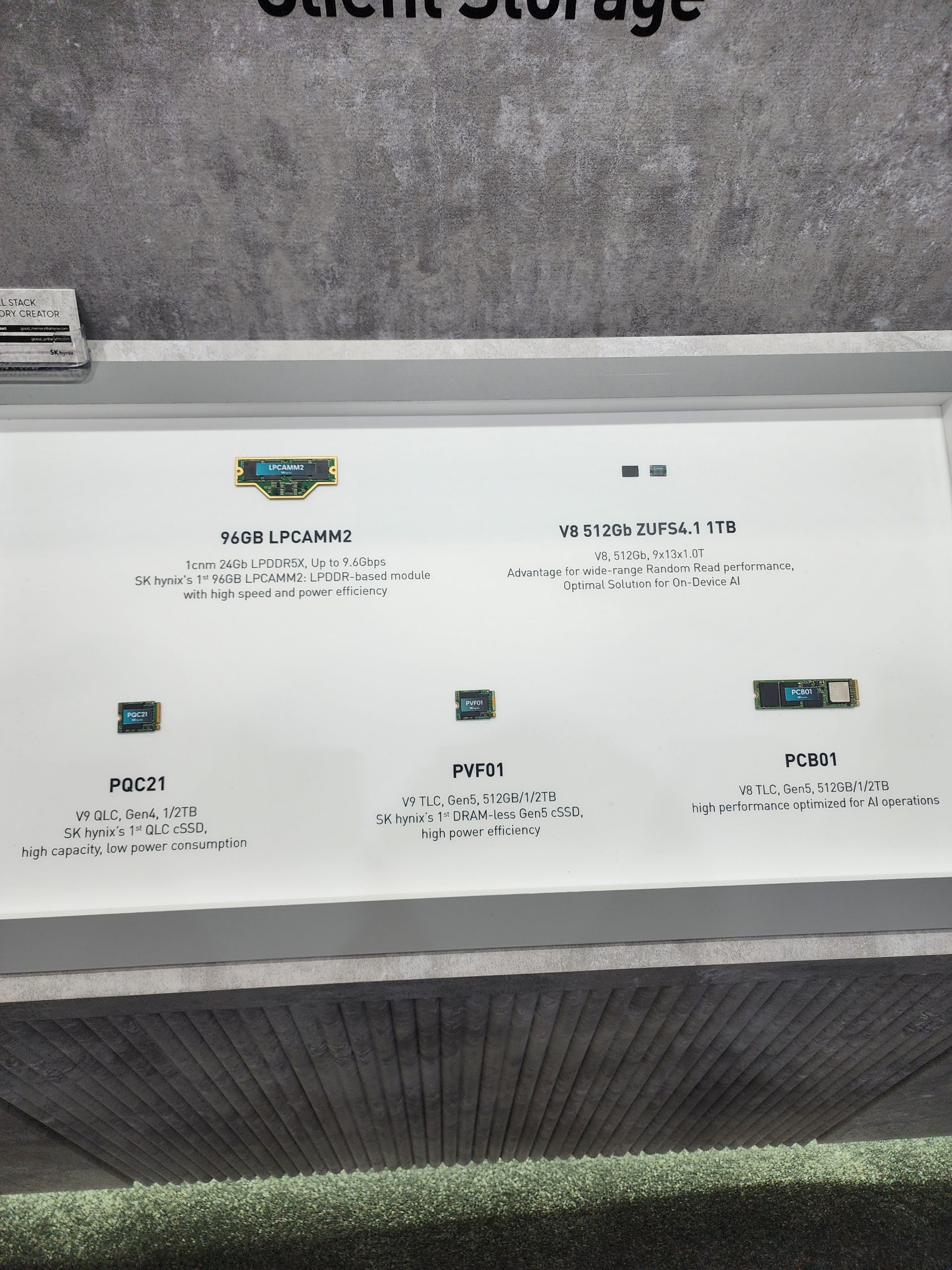
In terms of client and terminal-side products, SK Hynix also displayed a number of new products for "AI PC", including 96GB LPCAMM2 memory modules based on 1cnm process. The module adopts the LPDDR5X standard and has a transmission rate of up to 9.6Gbps. It is expected to be launched on the market later this year with the new generation AI PC platform. In the field of solid-state storage, the company exhibited the V9 NAND series, which is available in two particle forms: QLC and TLC. The capacity of a single chip can reach up to 2TB, and can be packaged into compact cSSD products. It focuses on miniaturization design and high energy efficiency, and adopts a DRAM-free architecture to further optimize cost and power consumption performance.
Overall, from HBM4E to stacked NAND, to high-density LPCAMM2 and V9 NAND SSD, SK Hynix demonstrated its complete storage layout around the two major application directions of AI data center and AI PC at this Computex. In the context of the simultaneous explosion of AI computing power and storage demand, a new generation of high-bandwidth, high-density, and low-power storage products will become a key support for GPU and other computing chips to release performance. The first public appearance of the HBM4E sample is also regarded as an important signal for the next round of HBM technology competition.