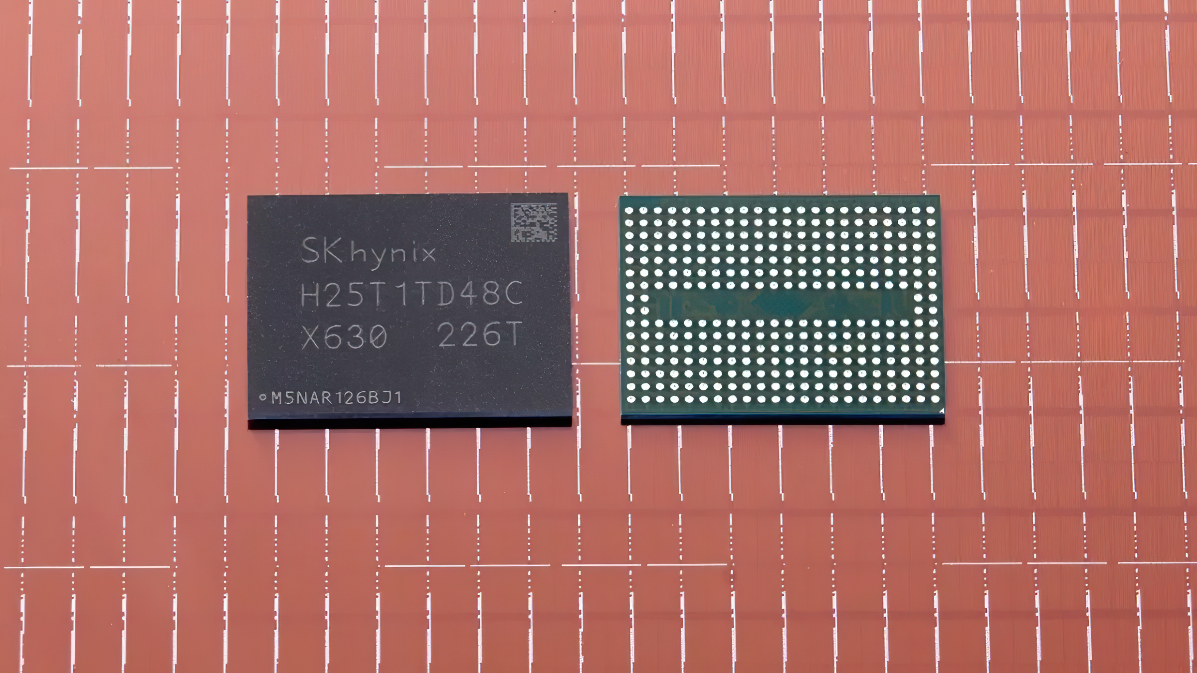
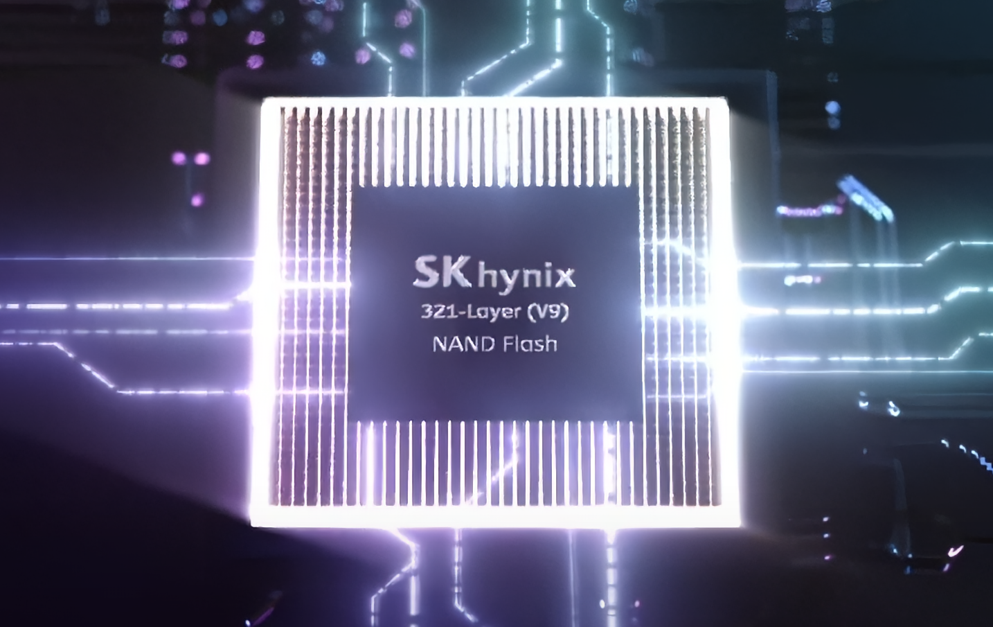
According to industry sources, SK hynix has completed the verification of its 375-layer NAND flash memory product and is expected to officially enter mass production in existing factories by the end of 2026 to meet the growing demand for storage capacity. These factories currently mainly produce 321-layer V9 NAND flash memory, and will support higher-layer stacking solutions through process conversion in the future.
SK hynix and Samsung are competing fiercely in the race to stack NAND flash memory layers. Samsung has previously revealed that it will increase the number of V-NAND layers to more than 400 layers through a dual-stack solution, and has demonstrated a technology roadmap that can reach up to 900 layers and target 1,000 layers. SK hynix has chosen to use 375-layer products as a phased node to enter mass production.
It is understood that SK hynix initially positioned this generation of products as "400-layer" NAND internally. However, during the actual process development process, due to serious process and signal transmission problems encountered when stacking too many layers in the same chip, the design was eventually revised to 375 layers. Industry sources revealed that the originally planned 400-layer product was adjusted to 375-layer, and subsequent roadmaps were extended to higher-stacked product nodes such as 480-layer and 604-layer.
To continue to move toward higher stacks such as 480 layers and 604 layers, it is no longer sustainable to rely solely on the existing material system. The report pointed out that SK hynix needs to make major adjustments in key conductive materials, gradually abandoning the currently commonly used tungsten (Tungsten) film, and switching to molybdenum (Molybdenum) as a new interconnect material to cope with the resistance and signal integrity challenges caused by high-level stacking.
In high-level 3D NAND structures, as the size of vertical wires and channels continues to shrink, the resistance of tungsten is difficult to control, and signal transmission loss and delay problems become increasingly prominent, becoming a "material ceiling" for continuing to increase the number of stacked layers. In contrast, molybdenum has better performance in high-resistance environments and can maintain better conduction characteristics under narrower wiring conditions. Therefore, it is regarded as one of the key materials to break through the limitations of high-rise stacking.
Samsung has taken the lead in introducing molybdenum materials in some of its NAND processes, and plans to further optimize its V-NAND production process this year and launch the first batch of 400-level products to consolidate its leading position in the high-end storage market. SK hynix will simultaneously complete the material switch from tungsten to molybdenum when following up with higher-layer products to narrow the gap in technology routes with competitors.
As the demand for storage capacity and performance in AI, cloud computing, high-performance terminals and enterprise-level data centers continues to rise, the continuous increase in the number of 3D NAND layers is regarded as a key direction to increase the bit density of a single chip and reduce unit storage costs. However, this also means that fabs need to invest more money in purchasing new materials, upgrading equipment and converting production lines to support more complex stacking and processing processes.
Taking molybdenum as an example, its demand has grown significantly in recent years and has become one of the important raw materials in the NAND supply chain. According to reports, Samsung purchased about 4 tons of molybdenum last year, and the purchase volume so far this year has increased to about 10 tons. With the introduction of molybdenum by manufacturers such as SK hynix, its usage is expected to reach about 4 tons this year.
Industry organizations predict that as 400-layer and higher-layer NAND enters the mass production stage, the market demand for molybdenum will rise rapidly: it is expected to reach 25 tons by 2027, 40 tons in 2028, approximately 60 tons in 2029, and further climb to 80 tons around 2030. In this process, material supply, cost control and technology iteration will jointly determine the competitive landscape of NAND manufacturers in the era of high-level stacking.
For SK hynix, the mass production of 375-layer NAND is not only a phased verification of its process capabilities, but also a technological springboard for the evolution to 480-layer, 604-layer and even higher layers. How to strike a balance between maintaining yield and cost, while successfully completing the migration of key materials such as tungsten to molybdenum, will directly affect whether it can occupy a favorable position in the competition with competitors such as Samsung.