According to people familiar with the matter, TSMC is developing a cutting-edge chip packaging technology called CoPoS, which stands for "Chip-on-Panel-on-Structure." This technology introduces glass material during the packaging process, which is used both as a temporary carrier and eventually becomes part of the substrate, forming a three-layer structure design similar to a "sandwich".
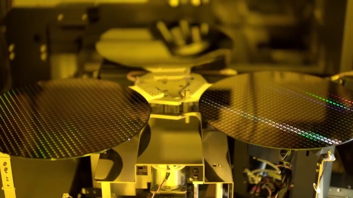
Reports indicate that TSMC plans to achieve mass production of CoPoS process chips as early as the end of 2028. With this new packaging solution, the manufacturing cost of related chips is expected to be reduced, and the performance will also be improved.
In terms of application implementation, Nvidia’s Feynman AI chip is expected to be the first product to adopt CoPoS packaging. The main target market of the new generation packaging technology is artificial intelligence and high-performance computing (HPC) chips, so it is regarded as one of the important basic supports for future high computing power platforms.
Industry analysts believe that if CoPoS ultimately proves to be disruptive, it will further consolidate TSMC's leading position in the global foundry and advanced packaging fields. This will also force competitors to accelerate the introduction of corresponding alternative technology solutions to cope with the pressure from TSMC in the dual dimensions of cost and performance.