The latest "300mm Fab Outlook" released by the global semiconductor industry association SEMI shows that investment in 300mm wafer fab equipment in the storage field is expected to exceed the US$50 billion mark for the first time in 2026, reaching US$52 billion, a year-on-year increase of 29%; by 2027, this number will continue to climb 11%, reaching US$57 billion. SEMI pointed out that this wave of capital expenditure growth is mainly due to the continued strong demand for advanced storage in the construction of artificial intelligence infrastructure, data centers and new generation computing systems.
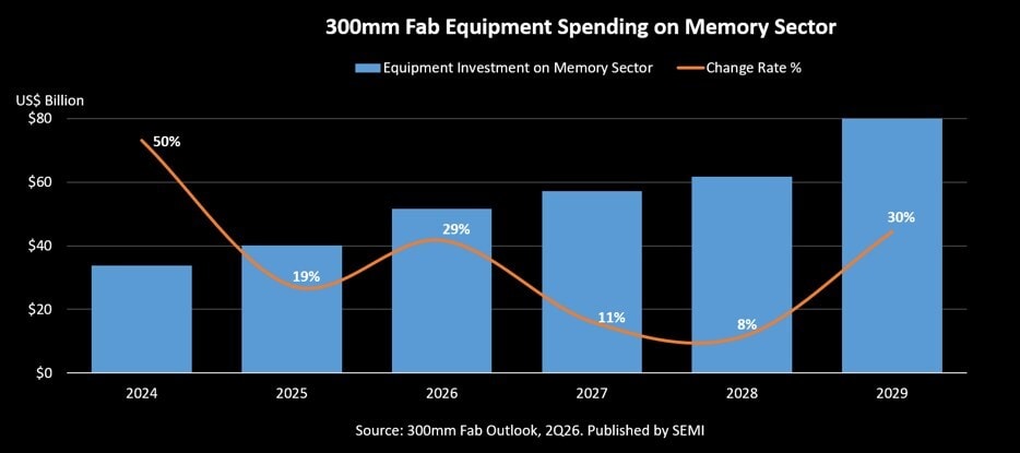
Looking forward to a longer period, the report predicts that global 300mm wafer fab equipment spending in the storage field will continue to rise at a compound annual growth rate of 19% from 2024 to 2029. At the same time, global 300mm storage capacity is also expanding simultaneously, and is expected to reach 4.1 million wafers per month in 2026, and further increase to 4.2 million wafers per month in 2027.
SEMI President and CEO Ajit Manocha said in the release that strong demand for high-bandwidth memory (HBM) and other advanced storage technologies is reshaping investment priorities across the semiconductor supply chain. He pointed out that with the rapid expansion of AI infrastructure, storage manufacturers are accelerating investment in capacity expansion and technology migration to support the arrival of the next wave of data-intensive applications.
In terms of specific segments, DRAM equipment spending is expected to increase by 29% in 2026, reaching US$37 billion, mainly driven by the strong demand for HBM and DDR5 in GPUs and various AI accelerators. Spending on 3D NAND equipment is also showing a strong upward trend and is expected to grow 28% to US$14 billion in 2026. Behind this is the continued rise in data storage demand related to AI deployment.
SEMI stated that continued investment in advanced process DRAM and higher-layer 3D NAND has further improved the prospects for future storage capacity, and raised relevant forecasts in the latest 2Q26 version of the "300mm Wafer Fab Outlook". However, the report also emphasizes that as advanced process DRAM, HBM and higher-layer NAND technology nodes continue to evolve, process complexity increases, and the technology migration process creates a certain restraint on effective production capacity growth, keeping production capacity growth overall "moderate and controllable."
The latest "300mm Fab Outlook" report covers a total of 413 wafer fabs and production lines around the world. Compared with the last release in March 2026, this update includes 155 data adjustments and 7 new wafer fab/production line projects. This data also reflects from the side that in the new round of semiconductor cycles driven by AI, the storage industry chain is in a stage of rapid expansion and upgrading, and the density and breadth of investment in related equipment and processes continue to increase.