Amkor Technology, a world-renowned packaging and testing company, recently officially started construction of a new semiconductor packaging and testing park in Peoria, Arizona. This rare local expansion project will cover multiple buildings and up to 750,000 square feet of clean rooms. The first factory is expected to be completed in mid-2027, and the entire park will be put into operation in early 2028.
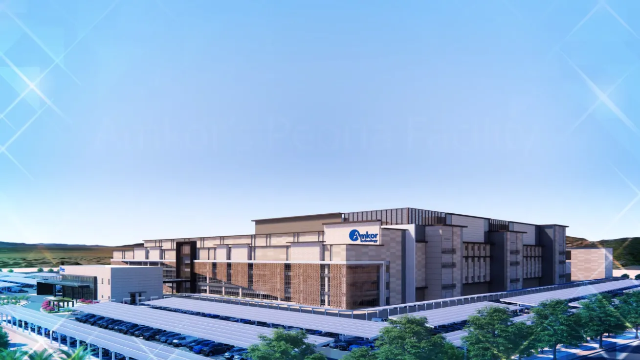
The facility has been identified to provide chip packaging services to leading companies such as Apple and Nvidia. Apple's own chips will be packaged here directly after being manufactured at the TSMC Arizona plant near the campus. The U.S. Department of Commerce has proposed up to US$400 million in financial support for this project through the CHIPS Act, calling it the largest outsourcing advanced packaging base in the United States, with an initial investment of US$2 billion. Local officials predict that the overall Amkor park investment scale may eventually expand to US$7 billion, creating as many as 3,000 related jobs.
TSMC is located in Arizona, which is less than an hour's drive from Amkor. It is simultaneously promoting three wafer fabs. Its future plans include 4-nanometer, 3-nanometer, and 2-nanometer production, all of which enjoy financial support from the CHIPS Act. The U.S. Department of Commerce emphasized that increasing domestic packaging production capacity is crucial to chip self-sufficiency, and the Amkor project is regarded as a key step in realizing the U.S.’s end-to-end chip manufacturing strategy. At the same time, Intel is also expanding its wafer production and advanced packaging capabilities through the bill in New Mexico and Arizona.
Advanced packaging is becoming a core link in the rise of high-bandwidth memory (HBM) and multi-chip architectures. U.S. officials have regarded packaging production capacity as a key weakness in the "fragile chip supply chain," especially products such as artificial intelligence accelerators that require extremely high integration and ultra-fast interconnection. The National Institute of Standards and Technology (NIST) believes that 2.5D packaging is the main bottleneck in the current production of AI chips and GPUs. Limited production capacity has led to product delays and insufficient supply.
Amkor's new Arizona campus responds head-on to this challenge, is designed for high-density integration, and is committed to serving as a bridge between U.S.-made wafers and finished AI systems. The project will attract technical talents from local universities and inject new impetus into Amkor's return to the U.S. manufacturing industry.