On April 23, 2026, NEO Semiconductor, a new American artificial intelligence and storage technology manufacturer, officially announced that its 3D X-DRAM technology has successfully completed the Proof-of-Concept (POC), proving that this new type of 3D stacked memory can be manufactured using the existing 3D NAND Flash production line, paving the way for high-density, low-power, and low-cost memory solutions in the AI era.
3D X-DRAM technology completes proof of concept, performance far exceeds existing standards
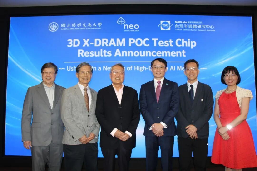
According to reports, this 3D X-DRAM technology proof-of-concept chip was developed by NEO Semiconductor in cooperation with the Institute of Industry-Academic Innovation (IAIS) of Taiwan Yang-Ming Chiao Tung University, and was tape-out and tested at the Taiwan Semiconductor Research Institute (NIAR-TSRI), an applied research institute. The chip successfully passed a comprehensive electrical and reliability evaluation, confirming the robustness and stability of its memory architecture.
According to the proof-of-concept test results released by NEO Semiconductor, 3D X-DRAM performs well on a number of key indicators. The specific data are as follows:
Read and write latency: less than 10 nanoseconds (<10 ns), which can meet the stringent speed requirements of high-performance computing;
Data retention time: more than 1 second at a high temperature of 85°C. This data is 15 times longer than the JEDEC (Solid State Technology Association) standard DRAM 64 millisecond retention time;
Bit line interference and word line interference: both exceed 1 second at 85°C, showing excellent anti-interference ability;
Cycle durability: more than 10¹⁴ read and write cycles, with extremely high service life;
This performance figure means that 3D X-DRAM far exceeds existing DRAM specifications in terms of data retention and durability while maintaining high-speed read and write capabilities.
Dr. Jack Sun, former TSMC chief technology officer and current senior vice president of Yang-Ming Jiaotong University, said: "I am very pleased that this close collaboration between industry and academia has verified the feasibility of the NEO 3D DRAM concept under real silicon manufacturing process conditions. This successful proof-of-concept not only demonstrates the potential of innovative memory architectures, but also confirms the feasibility of using mature processes to achieve advanced memory technology."
Jeongdong Choe, senior technical researcher at TechInsights, also pointed out: "As traditional DRAM scaling approaches its limits, NEO's silicon-based proof of concept represents an important milestone. Just like the transition to 3D NAND over the past decade, we are now witnessing the dawn of a new era of 3D DRAM that exceeds the limits of traditional scaling."
3D X-DRAM and X-HBM are expected to reshape the AI memory market
NAND Flash has already entered the 3D era, and the number of stacking layers is rising rapidly. More than 300 layers of NAND Flash are about to be mass-produced. This has also greatly improved the capacity ratio of 3D NAND Flash compared to the 2D era, and the cost per bit is also rapidly decreasing. In contrast, DRAM has remained stagnant for many years in the 2D plane era, and the cost per bit has been reduced very slowly.
While storage-class memory technologies like Intel's Optane 3D XPoint are being developed to offer speeds close to DRAM, the cost can also be closer to NAND. But Optane failed because its cost remained high because production could not be scaled up quickly, and its non-volatile memory was too complex to program.
Although stacking DRAM cells is an obvious architectural method to reduce DRAM costs and increase chip density, it also faces many challenges. However, NEO Semiconductor announced the launch of 3D X-DRAM technology in 2023, hoping to achieve this goal.
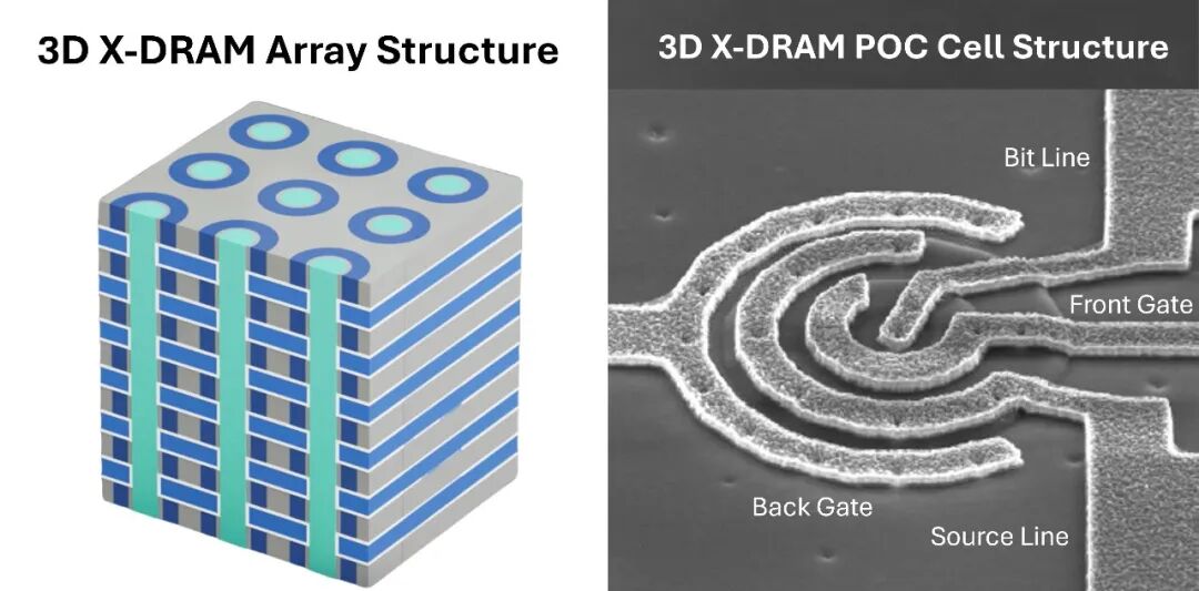
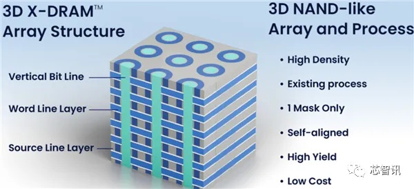
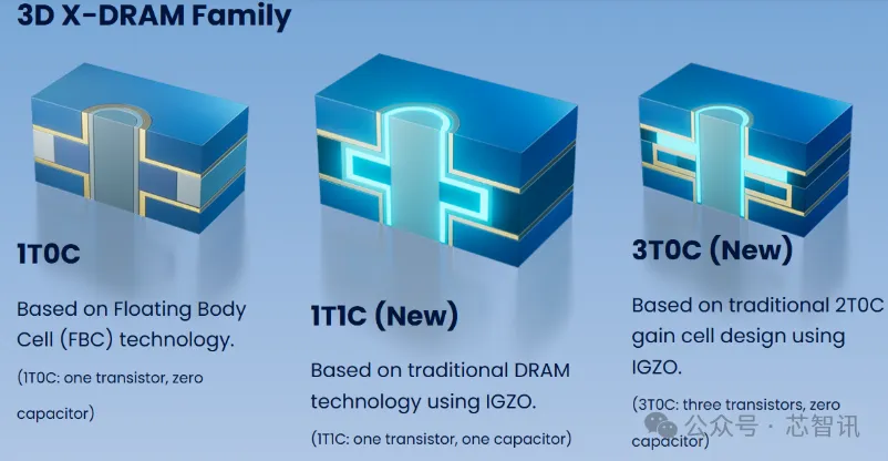
According to reports, the idea of 3D X-DRAM technology is similar to that of 3D NAND Flash, which mainly increases the memory capacity by increasing the number of stack layers. The first 3D DRAM unit design "1T0C" (one transistor, zero capacitor) launched by NEO Semiconductor in 2023 uses FBC floating gate technology similar to that in 3D NAND Flash chips, but adding a layer of Mask can form a vertical structure, which can achieve a 230-layer stack and a core capacity of 128Gb. The current core capacity of 2D DRAM memory is still 16Gb, achieving 8 times the capacity. Overall, this design has high yield, low cost, and greatly increased density.
In 2025, NEO Semiconductor launched 1T1C and 3T0C architectures, and announced that it will produce proof-of-concept test chips in 2026, with a density of up to 512Gb, which will provide 10 times the capacity of current traditional DRAM modules.
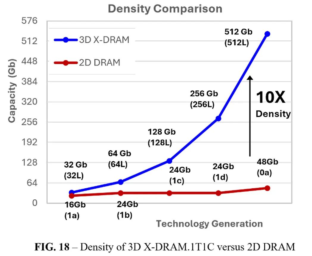
NEO Semiconductor also predicts that based on 3D X-DRAM technology, the capacity target of 1Tb for a single memory chip can be achieved between 2030 and 2035. This means that a single double-sided memory stick can achieve a capacity of 2TB, and server memory can achieve a single 4TB capacity using 32 chips. At the same time, costs will also be significantly reduced.
With NEO Semiconductor's 3D X-DRAM technology completing proof of concept this time, it also means that the technology is expected to be successfully commercialized.
More importantly, 3D X-DRAM can not only support high-performance, low-power workload requirements for AI, but can also be manufactured using 3D NAND Flash manufacturing processes, and can quickly utilize existing production lines to achieve large-scale mass production.
Andy Hsu, founder and CEO of NEO Semiconductor, said: "These results validate the new scaling path for DRAM. We believe this technology can achieve significantly higher density, lower cost and higher energy efficiency for the AI era. By leveraging mature 3D NAND manufacturing processes and ecosystems, we aim to make 3D DRAM a reality faster."
It is worth mentioning that NEO Semiconductor, based on 3D X-DRAM technology, will also launch the world's first ultra-high bandwidth memory (X-HBM) architecture for AI chips in 2025. This architecture claims to be able to achieve an ultra-high bit width of 32,000 bits (32K-bit) and a single-layer capacity of 512Gb. Compared with traditional HBM, the bandwidth is increased by 16 times and the density is increased by 10 times.
Today, as the demand for AI computing power increases exponentially, traditional HBM memory is also facing triple bottlenecks of density, bandwidth, and power consumption. Research by the Korea Academy of Science and Technology has predicted that even HBM8, which is planned to be launched around 2040, can only provide a 16K-bit bus and a capacity of 80Gbit per chip.
NEO's X-HBM has achieved a 32K-bit bus and a capacity of 512Gb per chip, which is equivalent to exceeding this performance prediction about 15 years in advance.
Received investment from the founder of Acer
Information shows that NEO Semiconductor is a high-tech company pioneering the next generation of artificial intelligence and storage technology. Founded in 2012 and headquartered in San Jose, California, the company is focused on redefining memory architecture to meet the growing demands of artificial intelligence and data-centric computing.
NEO Semiconductor founder and CEO Andy Hsu worked at an unnamed semiconductor startup for 16 years after receiving his master's degree from Rensselaer Polytechnic Institute in 1995. He founded NEO Semiconductor in August 2012 and is the inventor of more than 120 authorized patents.
NEO's key innovative technologies include X-NAND, 3D X-AI and X-HBM, as well as its flagship product 3D X-DRAM, a breakthrough architecture that leverages a 3D NAND-like structure to enable a scalable path to high-density, energy-efficient memory.
While the 3D X-DRAM technology successfully completed the proof of concept, NEO Semiconductor also announced that it has received a new round of strategic investment led by Stan Shih, founder of Acer and former director of TSMC. Shi Zhenrong has served as a director of TSMC for more than 20 years. His participation in this investment is regarded by the industry as a strong endorsement of NEO Semiconductor's technology and vision.
"I'm very pleased to see this breakthrough achieved through collaboration between industry and academia," said Zhenrong Shi. "This concept point was successfully realized by integrating innovation, strong engineering execution, and Taiwan's strong semiconductor ecosystem. NEO's 3D DRAM is expected to play a key role in future system architecture. As next-generation memory becomes increasingly critical for AI computing, innovations like 3D X-DRAM are expected to make a significant contribution to the development of the global memory industry."
NEO Semiconductor stated that the funds have supported the successful development of POC and will continue to advance the company's next phase, including array-level implementation, multi-layer test chip development, and deeper cooperation with leading memory companies to explore strategic partnerships.
NEO Semiconductor is currently in active discussions with industry partners in the memory and semiconductor ecosystem to advance this technology towards commercialization. With successful POC verification and growing industry participation, the company is entering a new phase focused on advancing 3D X-DRAM as a foundational technology for next-generation AI storage systems.