South Korean storage giant SK Hynix is cooperating with Intel and plans to introduce Intel's Embedded Multi-die Interconnect Bridge (EMIB) 2.5D packaging technology into high-bandwidth storage (HBM) products. As SK Hynix seeks to diversify its supply chain and more and more customers look to Intel Foundry as a candidate for advanced packaging, the storage manufacturer has begun R&D cooperation with Intel in the direction of 2.5D packaging.

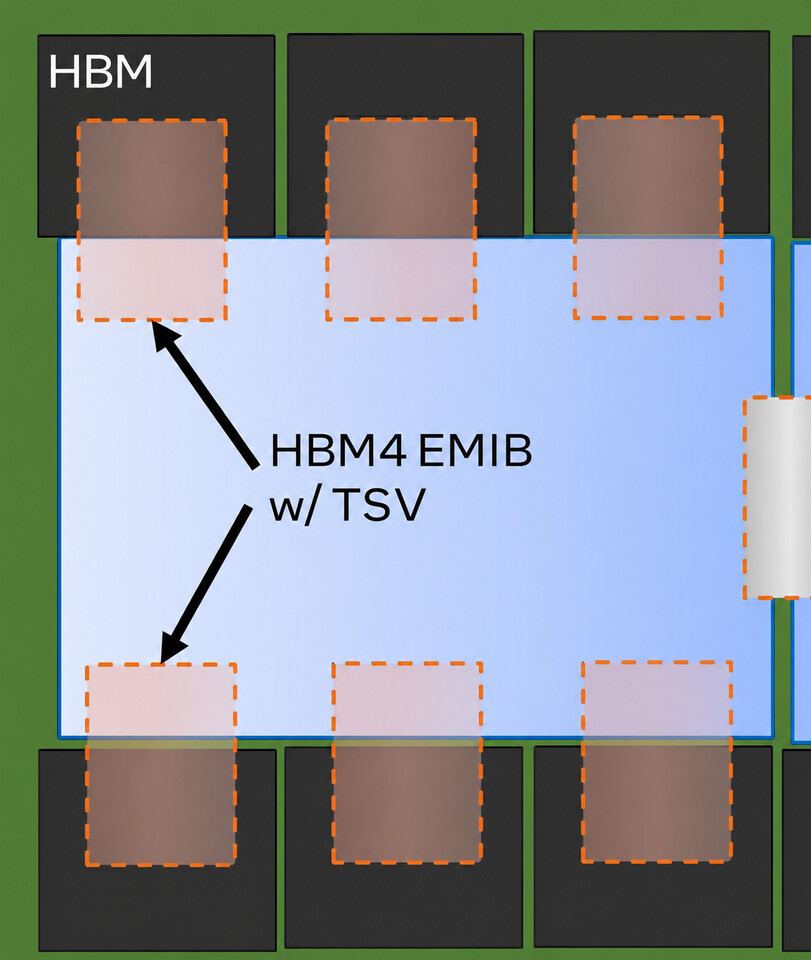
Intel's current main 2.5D packaging solution is EMIB, which achieves high-density interconnection between multiple cores by embedding silicon bridges in the packaging substrate. SK Hynix hopes to integrate this technology into its HBM product line, presumably focusing on making the new generation HBM4 meet EMIB integration requirements in structure and interface, so that it can seamlessly connect when its AI chip customers choose Intel fabs for advanced packaging of next-generation accelerators.
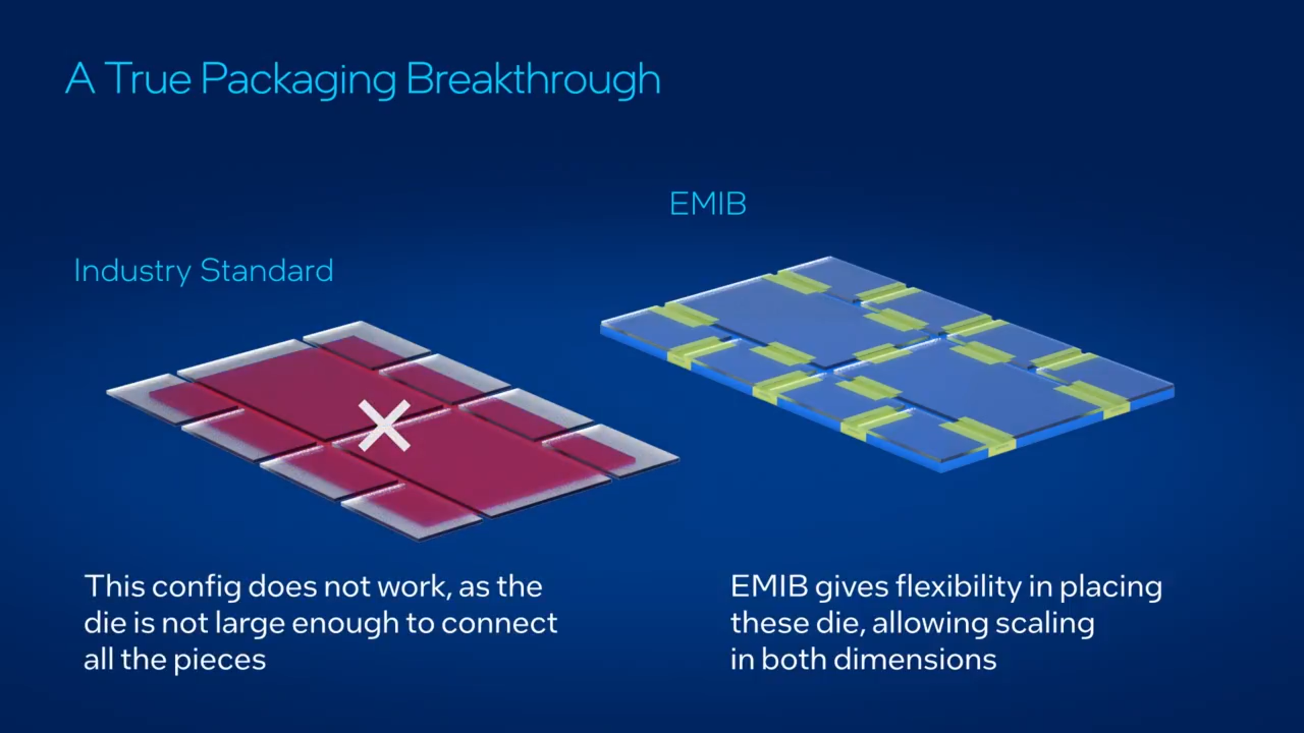
Previous reports have pointed out that Intel's small-size silicon bridge EMIB solutions, including EMIB-M with embedded metal-insulated-metal capacitors, and EMIB-T with through-silicon vias (TSV), provide relatively low-cost, extremely high shoreline density interconnection paths between logic chips and between logic chips and HBMs. However, so far, SK Hynix has relied on TSMC and its CoWoS 2.5D packaging technology for high-end AI packaging. As CoWoS gradually approaches its limits in terms of production capacity and process complexity, and customers begin to actively look for alternative advanced packaging paths, EMIB is becoming a powerful option to continue the core granulation route. It is expected to achieve expansion and stacking in more directions while exceeding the traditional 830 square millimeter mask area limit.
SK Hynix's DRAM and HBM chips are mainly manufactured in its own factories, but the company itself is not involved in complex system-level advanced packaging. The current most cutting-edge packaging form is hybrid bonding: directly stacking multiple pieces of silicon and completing vertical interconnections through thousands of TSVs. In the AI accelerator scenario, manufacturers need to integrate this HBM package with the GPU/dedicated acceleration core into a large package, which often involves more than ten such HBM packages on the same substrate. This is where TSMC’s CoWoS comes in, and Intel’s EMIB will soon join the fray to provide an alternative or parallel solution for the same high-density system-in-package needs.
It is unclear when the first products based on the combination of SK Hynix HBM and Intel EMIB will be available. What can be confirmed is that the joint research and development between the two parties on related 2.5D packaging and interface standards is already progressing, and the industry generally expects to see preliminary results or product launch signals in the next few quarters.