
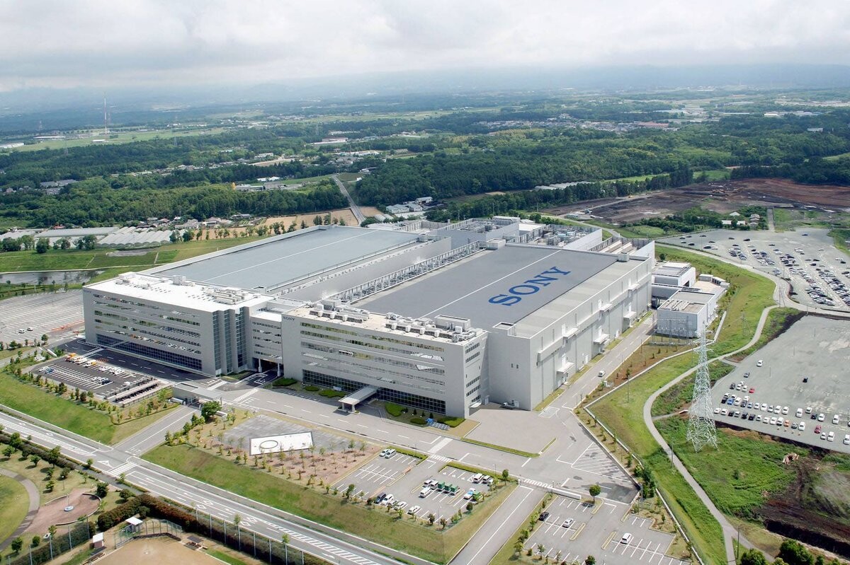
TSMC and Sony Semiconductor Solutions recently signed a non-binding memorandum of understanding to establish a joint venture to focus on the research, development and manufacturing of next-generation image sensors. In the future, the joint venture will be located in Sony's newly built wafer fab in Koshi City, Kumamoto Prefecture, Japan, with Sony holding a majority stake and assuming a controlling position. This collaboration will combine Sony’s deep accumulation in image sensor design with TSMC’s capabilities in advanced processes and mass production.
The cooperation goals of both parties are no longer limited to the traditional imaging market, but also target "AI in the physical world" application scenarios, including areas such as automotive electronics and robotics that require high-performance perception capabilities. As autonomous driving and smart industries place higher requirements on sensor performance, power consumption and computing power coupling, high-end image sensors are regarded as one of the key infrastructures for a new round of competition.
The specific investment scale of the joint venture is still under discussion. Sony is also considering additional capital expenditures at the existing Nagasaki factory. Both investments will be promoted in stages based on market demand and rely on the policy and financial support of the Japanese government. Reuters previously reported that Japan’s Ministry of Economy, Trade and Industry (METI) has confirmed that it will provide up to 60 billion yen in subsidies for Sony’s Kumamoto image sensor facilities, equivalent to approximately US$380 million, providing important financial support to the project.
From a time perspective, this cooperation has practical considerations for both parties. TSMC has already been deeply involved in the construction of the local semiconductor ecosystem through its first Kumamoto factory. The factory has entered the mass production stage at the end of 2024, providing 22/28 nm and 12/16 nm process chips for Sony Semiconductor Solutions and Denso (DENSO). On this basis, the new joint venture project is expected to push the cooperation between the two parties towards more advanced processes and higher value-added image sensor product lines.
For Sony, this move is also a proactive adjustment in response to intensifying competition in the image sensor market. Sony, which has long dominated high-end mobile phone camera sensors, is facing pressure from Samsung to obtain orders from major customers such as Apple, and its market share is being squeezed. Through in-depth binding with TSMC in manufacturing processes, production capacity and AI-related processes, Sony is trying to consolidate its voice in the field of high-end sensors and seize the opportunity in emerging needs such as automobiles and robots.
It should be pointed out that the two parties have only signed a non-binding memorandum of understanding at present, and the joint venture will not be formally established until a formal legally binding agreement is reached. However, under the premise that government subsidies have become clear, production line planning has gradually become clearer, and existing cooperation has a good foundation, this project is regarded as an important signal for Japan to continue to increase its investment in image sensors and AI hardware.