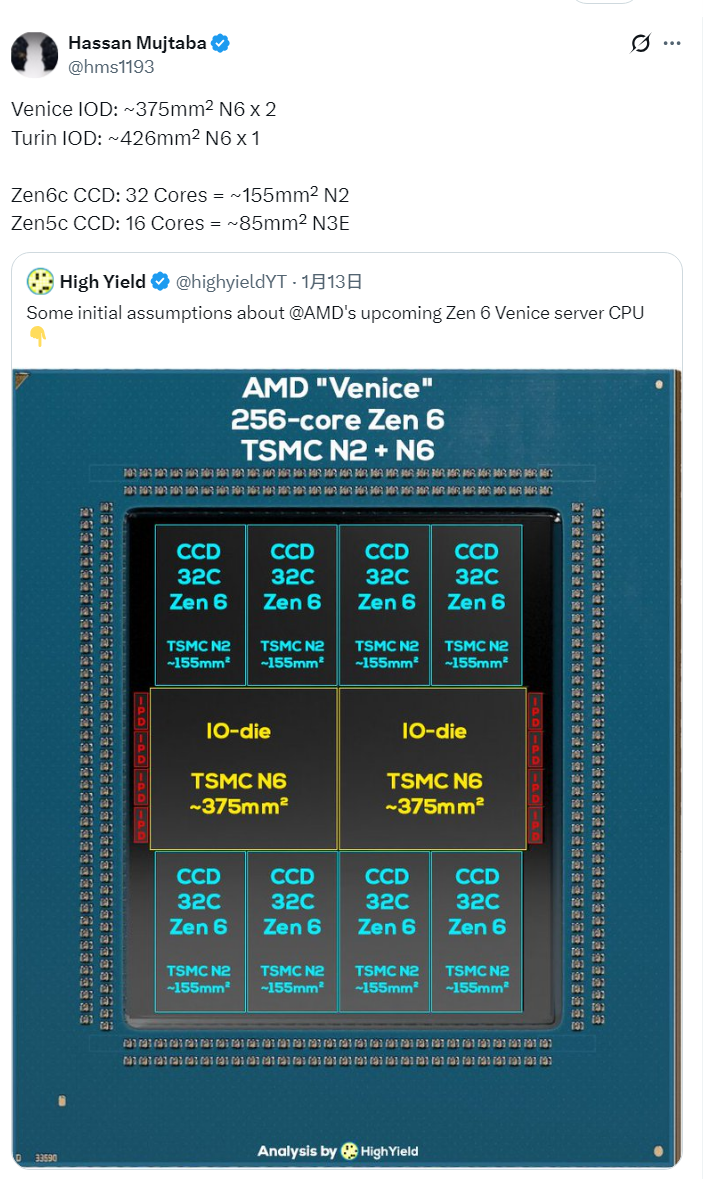
At this year's CES 2026 exhibition, AMD demonstrated the world's first new generation Zen6 EPYC Venice processor using TSMC's 2nm.Recently, new revelations have leaked online, revealing more structural details that have not yet been officially disclosed. AMD has pushed the number of cores to new heights on Venice, with the version of the Zen 6C architecture up to 256 cores. This design is achieved through a higher-density CCD and a new dual IO Die architecture.
Breaking information shows that the core improvement of EPYC Venice is mainly due to the new generation of Zen 6C CCD.Each Zen 6C CCD can accommodate 32 cores, which is directly double the 16-core design of the previous generation Zen 5C, allowing AMD to achieve a higher 256-core configuration while using only 8 CCDs.
In addition, the cache configuration has also been upgraded. Each Zen 6C CCD has a built-in 128MB L3 cache, making the total L3 cache capacity of the entire processor up to 1GB.
In terms of process strategy, EPYC Venice's CCD uses TSMC's 2-nanometer (N2P) process to pursue ultimate performance; while the IO Die responsible for I/O maintains a 6-nanometer process.
It is worth noting that EPYC Venice uses a dual IO Die architecture. The total area of the two IO Dies reaches 750mm², far exceeding the single IO Die design of the previous generation.
This means that the memory channel, PCIe and CXL expansion capabilities will be greatly improved, which is more conducive to supporting the dense deployment of GPUs and high-speed network devices in AI servers.