Samsung is making major structural adjustments to the power supply network of its new generation HBM4E high-bandwidth video memory to cope with the increasingly prominent power supply and heat dissipation engineering problems in the design of next-generation AI chips. This move comes just two weeks after the company announced that the world's first batch of HBM4 has achieved commercial shipments. At that time, the mass-produced product was able to operate stably at 11.7 Gbps, with speed redundancy reserved for sprinting to 13 Gbps.
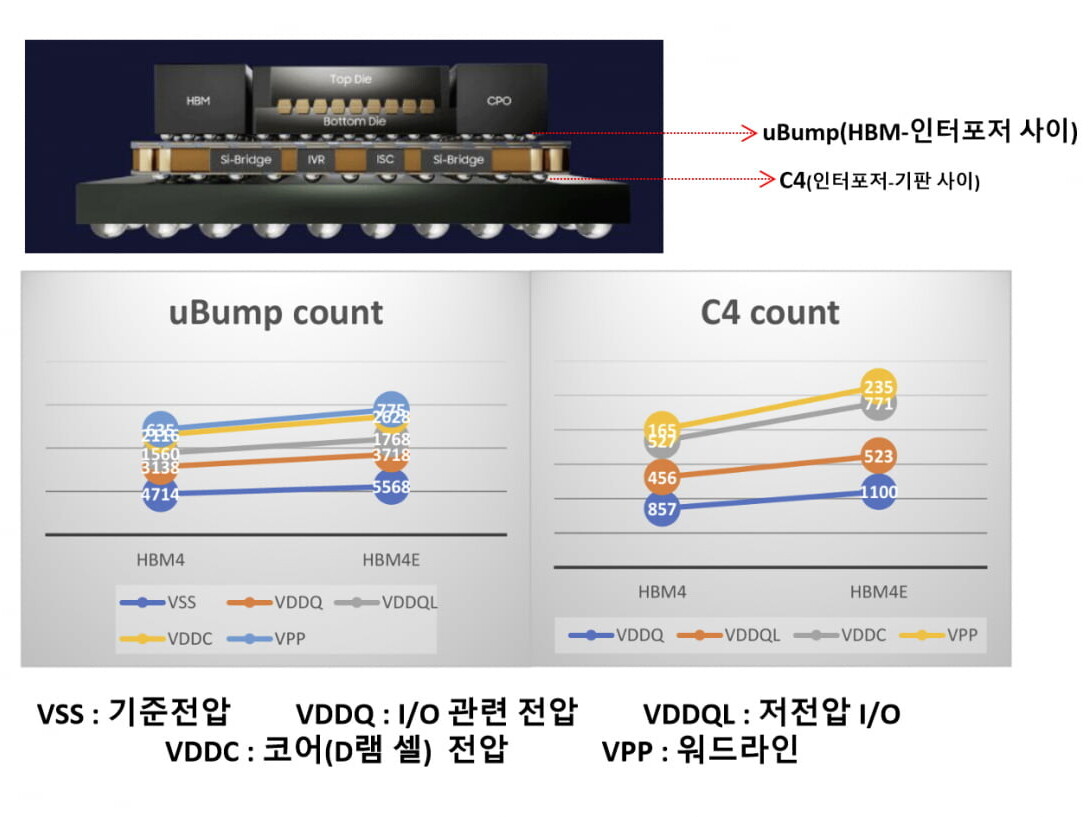
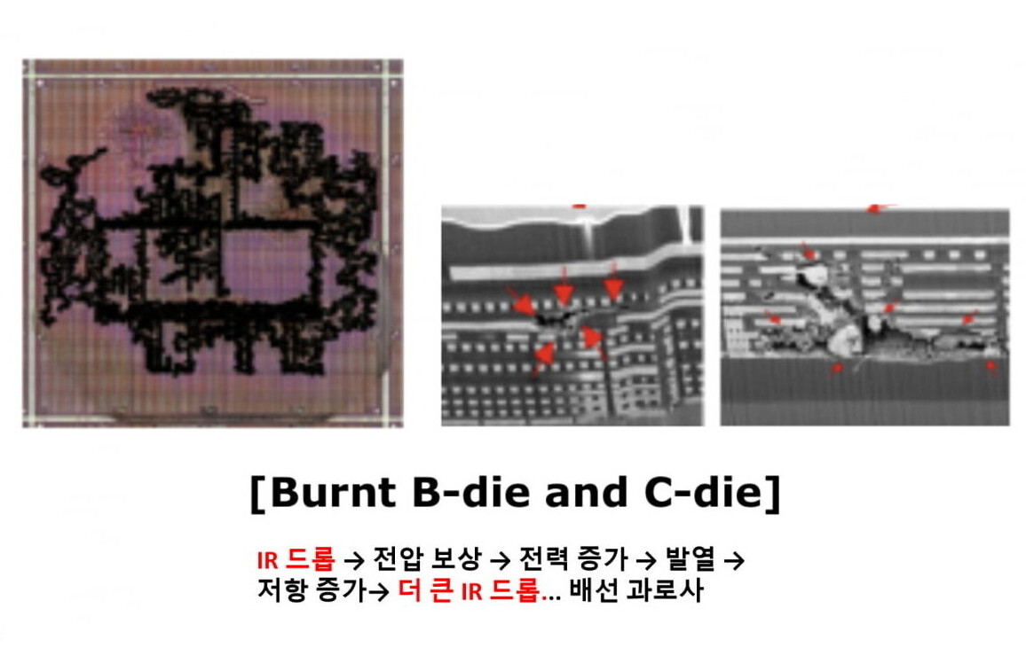
As the architecture evolves from HBM4 to HBM4E, the number of power supply solder bumps on a single chip increases from 13,682 to 14,457. However, it is still compressed into the same package area, and coupled with thinner and higher-density wiring, the current density and wire resistance increase simultaneously. The result is a more serious IR voltage drop inside the chip (the voltage gradually attenuates on the transmission path), forming a negative feedback loop under the superposition of heat, which not only affects performance, but may also cause local circuit failure.
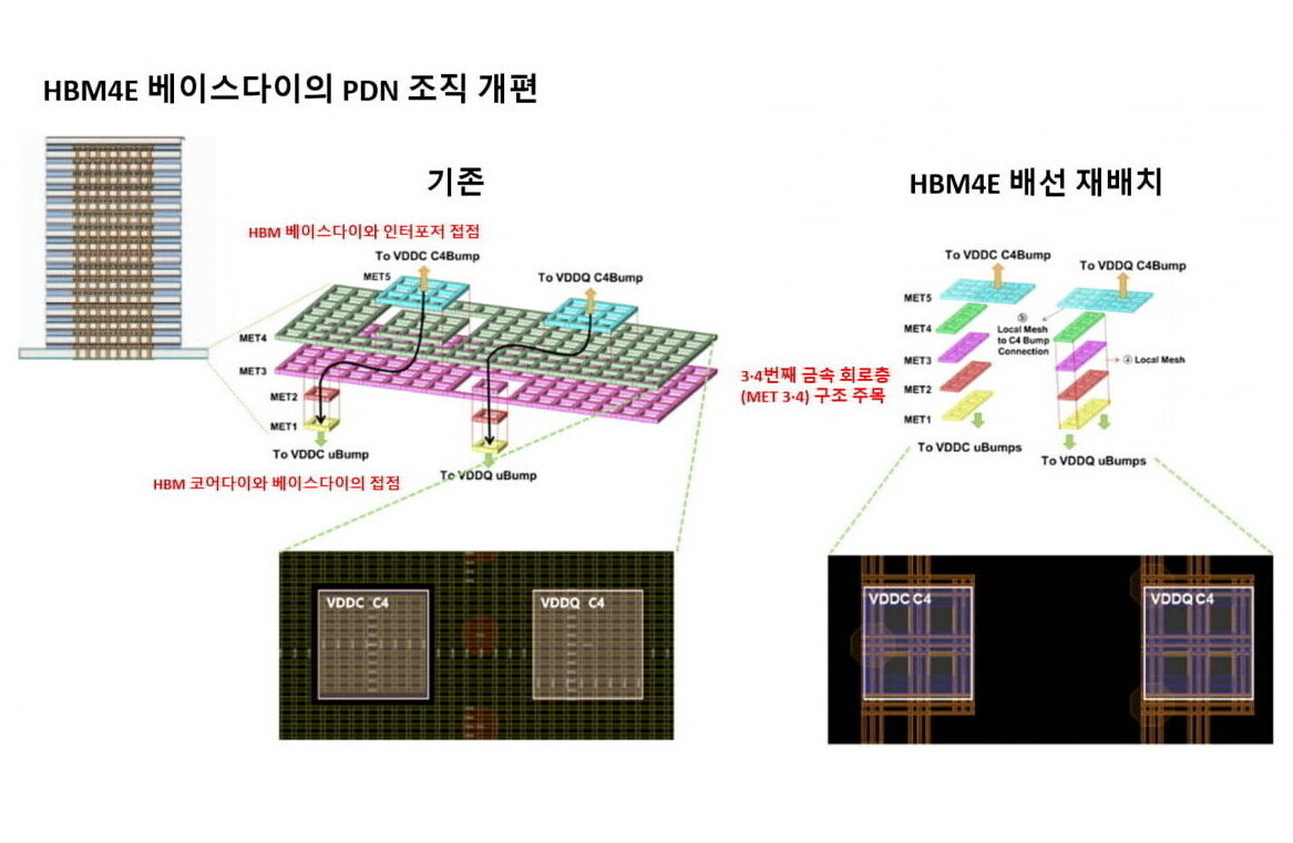
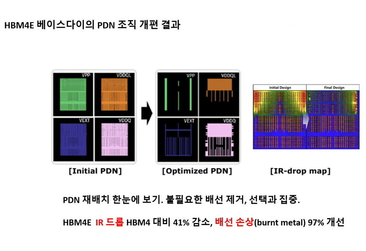
In order to break this power supply bottleneck, Samsung chose to "operate" on the power network structure itself. On the HBM base chip, the large-area honeycomb-shaped centralized MET4 power block originally located near the interconnect interposer was split into four smaller partitions, and the upper metal wiring layer was further scattered to shorten the critical path and alleviate local wiring congestion. An internal evaluation given by Samsung shows that after this segmented power network, the incidence of metal circuit defects has dropped by 97% compared to HBM4, and the IR voltage drop has improved by 41%, releasing more voltage margin for the chip to operate stably at higher frequencies, and also helping to improve overall reliability.
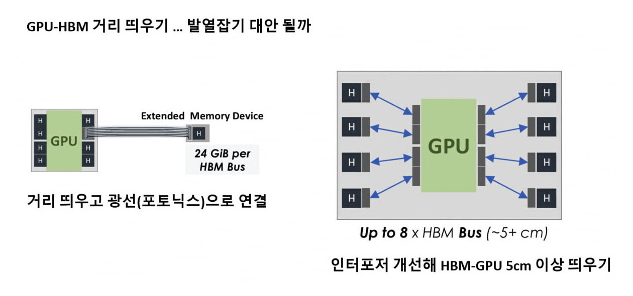
While "operating" on the power supply network, Samsung has also set its sights on a more radical system-level packaging evolution route-to completely "disassemble" HBM and GPU physically. One of the technical paths is to use photonic interconnection to maintain extremely high bandwidth over longer distances through optical signal transmission. According to reports, its theoretical transmission capacity can reach about 1,000 times that of existing copper interconnection, which is enough to make up for the loss in delay and bandwidth after the distance between HBM and GPU is widened. Samsung believes that with the continuous improvement of packaging substrate wiring capabilities, the distance between HBM and GPU is expected to be increased to more than 5 centimeters even without relying entirely on photonic interconnection. This will greatly alleviate the heat density and heat dissipation pressure caused by the close packaging of core computing chips and multi-layer HBM stacks in current high-end AI accelerator cards.
Industry analysts pointed out that in the context of the skyrocketing load of AI training and inference, HBM power supply and cooling have become key "stuck points" that restrict the continued linear expansion of computing power. Samsung's power network reconstruction on HBM4E and its forward-looking exploration of the HBM-GPU separation solution show its intention to take the lead in the next round of high-end graphics memory technology competition. The technical details of this time were initially disclosed by the Korean media "Korea Economy" and the market research agency TrendForce, and were subsequently confirmed by Samsung's relevant technical display materials.