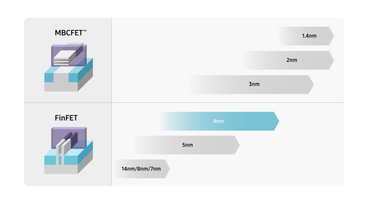
New reports from South Korea claim that Samsung Foundry has made key progress in the mass production of its 4nm FinFET process, and the yield rate has exceeded 80%, which means that the process has officially entered the process maturity stage. This node is seen as an important milestone for Samsung to catch up with rival TSMC in the field of advanced manufacturing processes.
The report pointed out that Samsung Electronics’ production base in Pyeongtaek Park not only mass-produces 5nm and 7nm chips, but also has the ability to supply 4nm chips on a large scale to customers in artificial intelligence accelerators, automotive electronics and mobile devices. This development will help Samsung compete more directly with TSMC for orders as demand for high-performance storage and computing chips from global technology giants reaches new highs.
Samsung's wafer foundry's current 4nm process is also the base chip process used by its sixth-generation HBM4 high-bandwidth memory chip. In scenarios such as AI training and reasoning, data centers, and high-end graphics cards, the demand for high-bandwidth storage such as HBM continues to rise, further increasing the strategic value of the stable and mature 4nm process to Samsung's overall semiconductor business.
Over the past six years, Samsung has continued to promote large-scale mass production of 4nm chips. The current yield rate exceeding 80% is regarded as a sign that the process has entered a mature stage, which is expected to buffer the impact of the recent surge in memory prices to a certain extent. The report predicts that with the improvement of 4nm production line yield and shipments, Samsung is expected to reverse its profit performance that has been pressured by rising storage prices in the second half of this year and push the semiconductor business back to a profitable track.