IBM and the U.S. Department of Commerce announced today that they have signed a letter of intent to build a quantum chip fab in the United States, aiming to consolidate the United States' leadership in global quantum technology and promote the country's rapidly developing quantum industry ecosystem. This plan will rely on CHIPS program incentive funds provided by the U.S. Department of Commerce to support IBM’s newly established company Anderon, which will become the first company in the United States to focus on quantum chip foundry. This move is regarded as one of the most significant commitments made by the U.S. government in terms of quantum research and industrial layout to date, with the goal of producing most of the world's quantum wafers in the United States.

According to published information, the U.S. Department of Commerce will provide $1 billion in incentive funds for the project through the CHIPS program, and IBM will also inject $1 billion in cash into Anderon, along with the transfer of important intellectual property, related assets, and professional technical teams. More external investors will be introduced in the future. Anderon will be headquartered in Albany, N.Y., and operate as an independent company building a 300mm quantum wafer fabrication facility. This project is designed to help the United States occupy a central position in the emerging quantum industry, which is expected to create up to $850 billion in economic value by 2040, while driving economic growth and improving national security capabilities.
IBM said that it combines the world's leading quantum computing research and development with mature wafer manufacturing experience to promote quantum chips from the laboratory to large-scale commercial use. IBM has developed and tested scalable quantum wafer technology, providing a clear path to commercialization. As a "pure foundry" quantum wafer fab, Anderon plans to provide wafer manufacturing services to many quantum technology companies around the world, making full use of IBM's technology accumulation in the construction and deployment of quantum computing systems.
U.S. Secretary of Commerce Howard Lutnick pointed out in a statement that through this investment in quantum computing research and development under the CHIPS program, the Trump administration is leading the world into a new stage of American innovation. These strategic quantum technology investments will strengthen the local industrial base, create thousands of high-paying jobs, and enhance U.S. quantum capabilities. Bill Fraunhofer, executive director of Semiconductor Investment and Innovation at the U.S. Department of Commerce, said that this incentive will enhance and accelerate U.S. leadership and technological resilience in the quantum field. Quantum computing is of great significance in defense, security, advanced materials, biopharmaceutical research and development, financial modeling, and energy systems.
IBM Chairman and CEO Arvind Krishna said that IBM has been deeply involved in the field of quantum computing for decades, and its experience in silicon wafer manufacturing will be the key to promoting the formation of a broader quantum technology ecosystem and will reshape the global innovation landscape and economic competitiveness. With the support of the U.S. Department of Commerce, Anderon is expected to become an important force in promoting the rapid development of the U.S. quantum industry. IBM plans to use its advantages in manufacturing equipment and expertise to help Anderon build a secure, U.S.-based quantum wafer supply chain to serve multiple hardware suppliers.
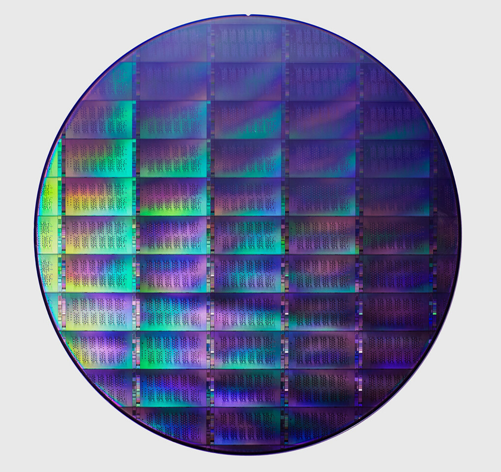
On the technical path, Anderon will initially focus on supporting the production of superconducting qubits and supporting electronic device wafers, with subsequent plans to expand to more quantum technology forms. Since its establishment, the company has been positioned as the "anchor" of the U.S. national-level quantum wafer manufacturing ecosystem, ensuring that IBM and other quantum companies can achieve large-scale quantum technology production in the United States. Its planned advanced 300mm wafer process will cover a series of cutting-edge technologies including superconducting wiring, through silicon vias and bump connections, and will be equipped with a mature process design suite, online wafer testing and characterization capabilities, and a complete mass production process to support rapid iteration and reliable expansion.
The announcement pointed out that quantum computing is a new paradigm that is completely different from traditional computing and is expected to solve problems that are difficult for traditional supercomputers to deal with in fields such as materials science, chemical research, complex optimization and network security. Driven by IBM, the United States currently maintains a leading position in this field, but it still needs to accelerate the pace of hardware development to meet the needs of the growing industrial ecosystem and maintain global economic competitiveness and national security advantages in the coming decades.
To date, IBM has deployed more than 90 quantum systems, more than all other companies in the world combined. The company's global customer and partner ecosystem covers more than 325 Fortune 500 companies, startups, universities and government agencies, which are using IBM's quantum computing platform to address cutting-edge scientific challenges in chemistry, biology, materials science and other fields. IBM has also cooperated with the National Institute of Standards and Technology (NIST), the Defense Advanced Research Projects Agency (DARPA) and multiple laboratories under the Department of Energy for many years. It is at the core of building a safe and reliable domestic quantum manufacturing system in the United States, and plans to launch the world's first large-scale, fault-tolerant quantum computer for commercial customers by 2029.
It should be noted that the official implementation of Anderon still depends on further negotiations between IBM and the U.S. Department of Commerce based on the current letter of intent and the signing of the final agreement document. Once the relevant procedures are completed, this quantum fab project will mark a critical step in the construction of quantum computing infrastructure in the United States.