Morgan Stanley's latest research shows that the current defect density (D0) of Intel's next-generation 14A process node is about 0.5, which means that in the long and complex semiconductor manufacturing process, the proportion of purely functional scrapped chips produced per unit area of wafers is low, and the overall yield level is considerable compared to new processes at the same stage.
For Intel, this data shows that 14A is still in the early stages of its ramp-up, but supports previous claims that 14A has surpassed 18A on the same development schedule. Intel plans to further reduce the defect density of this node to about 0.1–0.2 in the first quarter of 2027, and use this as a node to start internal test chip tape-out and small-scale mass production ramp for its own products, and then enter the risk trial production stage in 2028, and enter large-scale mass production in 2029.
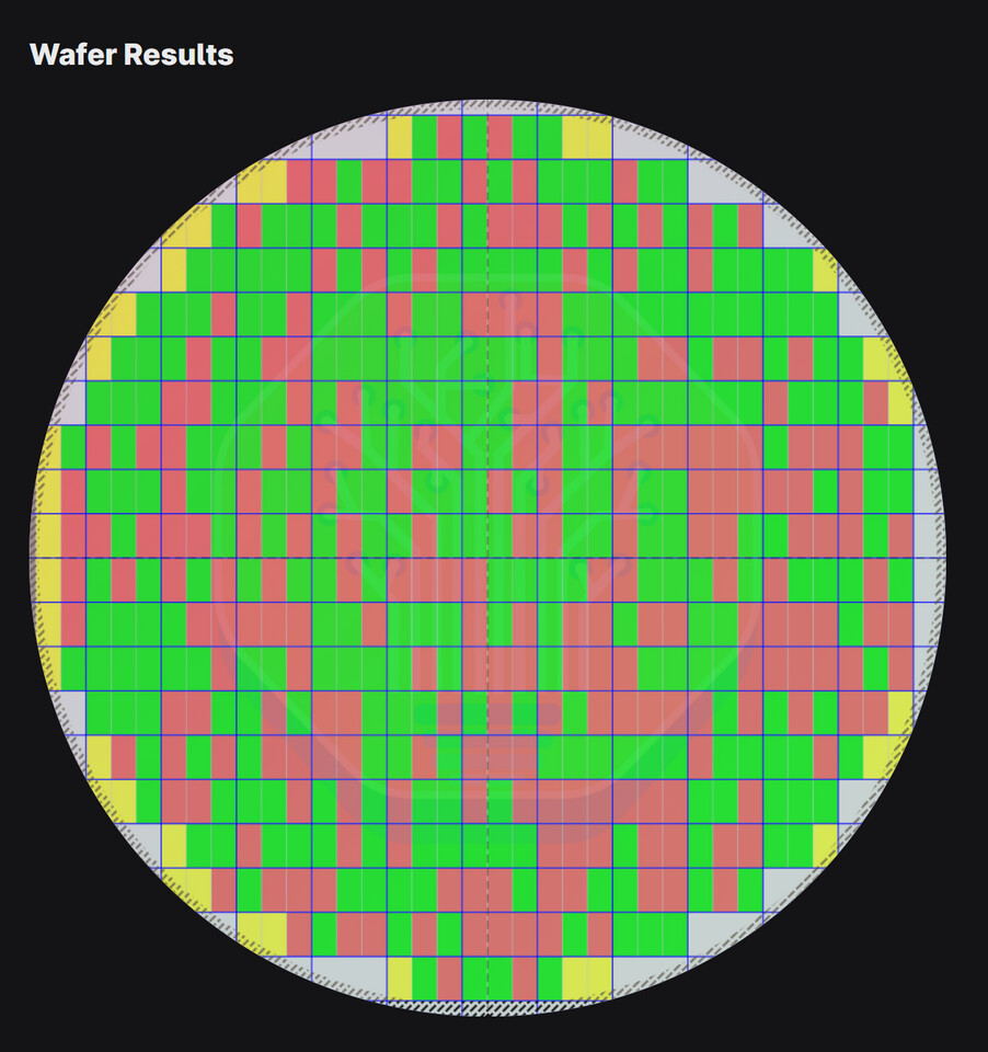
In terms of current mass-produced products, Intel's latest "Panther Lake" SoC uses a multi-chip packaging solution, in which the computing chip (compute tile) used for the computing core is manufactured based on the 18A process. Its die size is approximately 8.004 × 14.288 mm and the area is approximately 114.304 square millimeters. The article uses this as a reference, assuming that the die area remains unchanged, but the transistor density is increased and migrated to the 14A process. Under the current condition of D0=0.5, the theoretical yield of a design of this size on the 14A process can reach approximately 56.45%. It should be emphasized that 18A is currently in the high-volume production stage, so the actual yield is still better than 14A, which is still in the ramp-up period. However, from statistical estimates, 14A can reach this level with the current process maturity, which is considered a quite positive signal. This estimate is based on production conditions on a high numerical aperture (High-NA) EUV device in half-field exposure mode and reflects the early stages of sustainable optimization for Intel 14A. Morgan Stanley also mentioned in the report that the yield rate of test chips currently used for verification is about 40%. Considering that the die size of the test chip is likely to be significantly larger than the "Panther Lake" computing chip, this data is not inconsistent with the above model estimate.
From a mid- to long-term goal, if Intel can successfully compress the D0 defect density of 14A to 0.1–0.2, then for a chip design with an area of about 100 square millimeters, its theoretical yield is expected to increase to 80%–90%. The specific level depends on the actual circuit structure and layout implementation. The report pointed out that this prediction is mainly based on the classic Poisson yield model, and there are many different calculation methods in the industry; in addition, it is necessary to distinguish between "defect yield" and "parametric yield" - the former focuses on whether the chip can light up and work, and the latter considers whether the chip can fully meet product specifications in terms of power consumption, frequency and other indicators. Parametric yield is often highly sensitive internal data, and it is difficult for outsiders to obtain detailed information about 14A in this regard.

In terms of design support and customer ecosystem, Intel 14A currently corresponds to version 0.5 of the Process Design Kit (PDK). According to the plan, when version 0.9 PDK is released, foundry customers will finalize the mass production scale, specific product design and other key parameters on the platform. Lip-Bu Tan, a member of Intel's board of directors and a veteran investor in the industry, previously called the 0.9 version of the PDK the "holy grail" of this node and expected that this version would be open to the public in October this year.
In terms of production line equipment and process capabilities, Intel's cooperation with ASML has completed the acceptance test of the High-NA EUV lithography machine corresponding to the 14A node in Intel's foundry business production line to improve the overall wafer output capability. The currently deployed TWINSCAN EXE:5200B is ASML’s second generation High-NA EUV scanning device, inherited and upgraded from the TWINSCAN EXE:5000 platform previously used for the 14A trial run. With these new generation equipment, Intel has completed more than 30,000 wafer processing experiments in a single season, and by reducing the photolithography steps required for specific process layers, the process of some layers has been reduced from about 40 steps to less than 10 steps, thereby significantly shortening the process cycle time and simplifying the overall manufacturing process.
Against the background of the fierce competition in global wafer manufacturing, Intel's phased breakthrough in 14A process yield not only lays the foundation for the company's own future product roadmap, but also provides an important bargaining chip for its foundry business to win orders from potential large customers in the High-NA EUV era. The yield estimation model cited in the report comes from the wafer and die yield calculation tools provided by SemiAnalysis, which further supports the current analysis and judgment of 14A production capacity and yield prospects.