Intel's latest generation manufacturing node 18A has entered a stable mass production stage after experiencing yield issues for several months. According to the latest research report from the sell-side organization BlueFin Research Partners, the current defect density of 18A has approached the low end of the D0=0.1 to D0=0.2 range common in mature processes, which means that it has sustainable high-capacity conditions in terms of both manufacturing and cost.
BlueFin pointed out that the yield bottleneck that has plagued 18A in the past few months has been solved by Intel, turning the production line of this key node from "conquering yield" to "stable production". Intel said late last year that 18A yields were improving at a rate of about 7% per month, and today's improvement trajectory is basically in line with expectations at the time. With the introduction and mass production of the first 18A product Panther Lake processor, continuous process optimization has pushed this node into a more mature and stable operation stage.
Currently, 18A mass production is mainly concentrated in Fab 52 in Phoenix, Arizona, and a factory in Hillsboro, Oregon. The two places have a combined monthly production of about 30,000 wafers. At this stage, this production capacity can basically cover Intel's internal needs, including its own products including Panther Lake. However, as more products shift to the 18A process, Intel needs to continue to expand its overall production capacity layout. At the current stage of development, 18A still mainly caters to Intel's own products. The company is promoting process optimization while planning subsequent capacity expansion and node evolution.
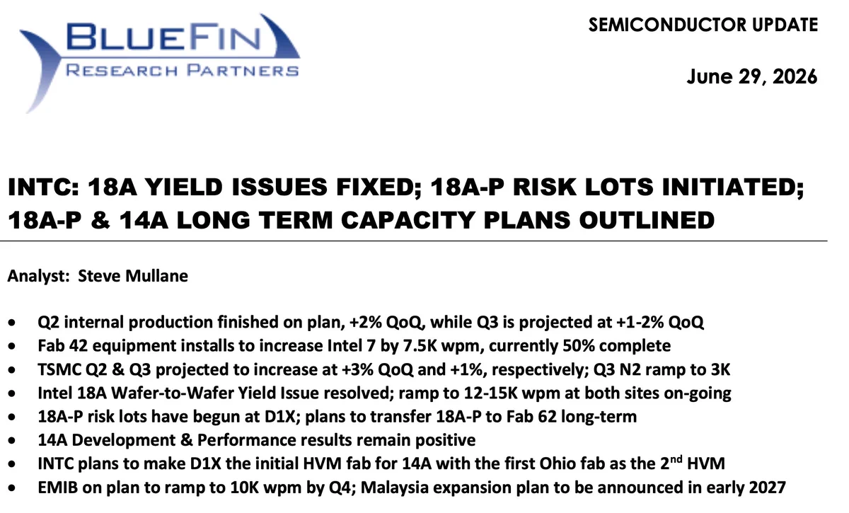
Meanwhile, Intel has started risky trial production of 18A-P at its D1X factory in Oregon, a new version considered an evolution of the original 18A process. According to the plan, after 18A-P completes its verification, it will be transferred to Fab 62 as a long-term high-capacity production base. People familiar with the matter revealed that when facing external foundry customers, Intel’s roadmap will focus on 18A-P, 18A-PT and the subsequent 14A nodes, of which 18A-PT will be paired with 18A-P to form a process combination for different customer needs.
After 18A, Intel also began to lay out the next-generation 14A process. The early results from sample production are considered "optimistic", which enhances the company's confidence in the advancement of research and development of this node. Intel plans to use the D1X factory to undertake the initial large-scale production of 14A, and then use the new facility in Ohio as a second production base to provide redundancy and expansion space for the full rollout of the node. 14A risk trial production for external customers is expected to start in 2028, with high-volume production targeted for 2029.
From a timeline perspective, the continued improvement of 18A yield, the mass production of Panther Lake, and the launch of 18A-P and 18A-PT mark Intel's overall shift in advanced processes: from overcoming technical difficulties to gradually moving toward steady-state mass production and foundry market layout. With the advancement of the 14A node and the rollout of multi-site capacity in the United States, Intel is trying to re-consolidate its technology and market voice in the fierce semiconductor manufacturing competition with a complete set of process and capacity planning from 18A to 14A.