GlobalFoundries officially announced today that it has signed a letter of intent to cooperate with the U.S. Department of Commerce. According to the agreement, GlobalFoundries will receive US$300 million in subsidies from the U.S. CHIPS Act fund pool, and the U.S. government will also use this to obtain approximately 1% of GlobalFoundries' equity.
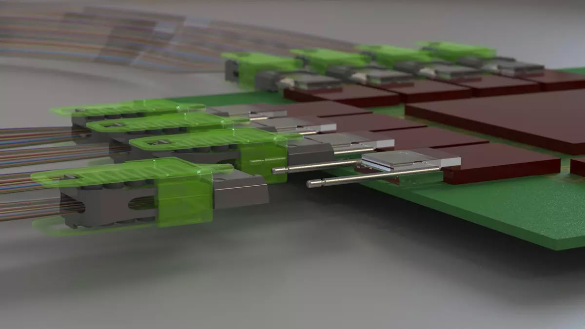
Since GF decided to abandon the R&D and manufacturing of advanced processes during the industry's transition to 7-nanometer processes, its business focus has gradually shifted to other specific technology areas with high added value. With the rapid expansion of the field of artificial intelligence, silicon photonics technology that combines photonics and semiconductors is showing great commercial and strategic value.
GlobalFoundries stated that the US$300 million in R&D funds received this time will be fully invested in the development of next-generation silicon photonics technology and advanced packaging processes. The core areas include near-package optics (NPO), co-package optics (CPO), 3D hybrid bonding, and new material research and development. Previously, GF had just launched a co-packaged advanced optical engine platform called SCALE, which supports single-channel 400 Gb/s high-performance data transmission. GlobalFoundries plans to use the funds to upgrade its manufacturing sites in Malta, New York, and Burlington, Vermont, to fulfill its commitment to promoting the localization of key semiconductor technologies.
The project has also received strong support from many technology giants. Many SCALE platform partners, including AMD, Broadcom, Cisco, Corning, Lumentum, Meta, Microsoft, NVIDIA and Qualcomm, have made public statements. Companies generally believe that when traditional copper cable transmission encounters physical limits, using photons to replace copper cables for high-speed data transmission is the key to breaking the situation, and they affirm the strengthening of the US domestic supply chain in the field of silicon photonics.