
Abstract:
GlobalFoundries (GF) announced the FDX Fusion fully depleted silicon-on-insulator (FD-SOI) process route, aiming to provide low-power, highly integrated chips for "physical AI" equipment such as robots, automobiles, and industrial automation. The company said the first generation of FDX Fusion is expected to achieve "7nm-level digital performance" and plans to start manufacturing at its Dresden, Germany, factory in 2028.
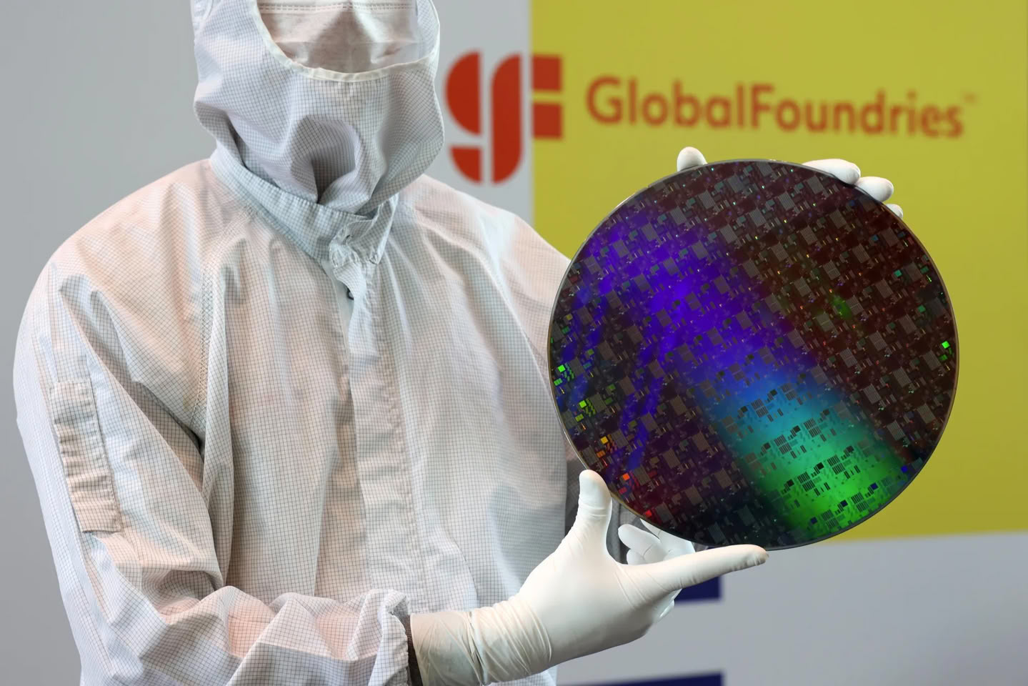
This statement refers to the digital logic performance level and does not mean that GF has resumed the 7nm FinFET process that was suspended in 2018, nor can it be directly equivalent to the 7nm process node or transistor density of other fabs.
FDX Fusion continues GF’s FD-SOI route. This technology sets an insulating layer under the silicon layer and supports back-bias adjustment, which can be adjusted between power consumption and performance according to the workload; GF said it helps reduce leakage, optimize energy efficiency, and is suitable for integrating radio frequency, analog and digital circuits. The new platform is also planned to incorporate embedded non-volatile memory, in-memory computing and high-density logic. The indicators announced by GF include that the ft/fmax of the radio frequency device can reach up to 0.5 terahertz, and the density of the first-generation FDX process has increased by more than twice; the company has not yet released enough detailed design data for external independent verification. The 0.5 terahertz here is an indicator of the radio frequency device, not the operating frequency of the chip processor.
GF positions this process in physical AI, that is, applications where devices sense the environment locally, process data and respond in a timely manner, including edge reasoning, sensor fusion, robotics, automation equipment, automotive electronics, autonomous systems and intelligent connected devices. Its design focus is not simply on pursuing the smallest transistors, but on trying to integrate sensing, computing, wireless communications, control and storage in the same platform to reduce system complexity, latency and power consumption. GF said it has carried out early evaluations with some customers, but has not yet announced specific chip products or mass production customer orders.
According to the company's roadmap, the FDX Fusion demonstration chip is expected to be delivered to customers for evaluation in early 2027, the first version of the process design kit is planned to be available in mid-2027, and the mass production target is 2028. GF also explained that the development of the Dresden FDX Fusion project still depends on whether the German federal government approves the upcoming IPCEI advanced semiconductor technology project, so the roadmap still has policy approval conditions.
This route is not the same as the project that GF suspended in 2018. At that time, the company shelved the research and development of 7-nanometer FinFET on the grounds that it would concentrate resources on more distinctive processes and markets; the newly announced FDX Fusion is based on FD-SOI and focuses on low-power consumption, radio frequency, and mixed-signal integration. GF is also advancing a 1.1 billion euro SPRINT expansion plan in Dresden, with the goal of increasing the plant's annual production capacity to more than 1 million 300mm wafers by the end of 2028; this capacity expansion covers the entire business of the plant, not all of it is used for FDX Fusion.
Comments