
Abstract:
The Logic Folding chip architecture proposed by Huawei in recent years has once again attracted the attention of the semiconductor industry. Data previously released by Huawei shows that by reorganizing the internal logic circuits of the chip and conducting a vertical three-dimensional layout, the signal transmission path can be significantly shortened and the number of buffers required for the clock network can be significantly reduced. However, semiconductor industry experts point out that although this architecture can reduce some signal transmission costs, it cannot fundamentally solve the most difficult heat dissipation problem of 3D chips, and this may also become a major obstacle to further expansion of its scale.
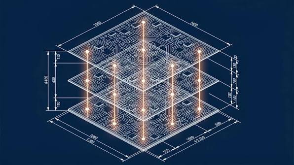
Logic Folding is a chip design method proposed by Huawei in the context of restrictions on advanced semiconductor technology in the United States. The core idea is not to simply rely on more advanced photolithography processes to shrink transistors, but to shorten the propagation distance of signals inside the chip by rearranging the logic units inside the chip and moving the circuits that were originally mainly distributed on the two-dimensional plane to the vertical direction.
This idea is based on the "Tau Scaling Law" proposed by Huawei. Traditional Moore's Law mainly focuses on transistor size and number of transistors, while Tau Scaling proposed by Huawei pays more attention to signal propagation time and internal chip interconnection distance, hoping to improve performance and energy efficiency by shortening the data transmission path.
In the test data released by Huawei, Logic Folding can significantly shorten some critical logic paths. Among them, the clock network is one of the key optimization targets. Since modern high-performance processors contain a huge number of logic units, clock signals must be propagated to various areas of the chip through complex clock trees, and in order to ensure signal quality, a large number of clock buffers need to be deployed.
Huawei data shows that after reorganizing related circuits through Logic Folding, the number of clock buffers in a processing module can be reduced from approximately 43,600 to 19,000, a reduction of more than 50%.
At the same time, the length of the relevant clock wiring can also be significantly shortened. According to data released by Huawei, the critical path in some designs can be shortened by up to 70%, and the overall signal path can be shortened by about 20% on average.
The principle behind it is not complicated. The longer the signal lines inside the chip, the greater the parasitic resistance and capacitance, and the more energy required to drive these lines. By shortening the signal propagation distance, the capacitive loading created by the interconnect can be reduced, thereby reducing dynamic power consumption.
Clock networks are particularly suitable for this optimization because clock signals need to be continuously propagated throughout the chip. Even if the processor isn't performing a lot of actual computation, the clock tree can still consume considerable power. Therefore, if the number of clock buffers and associated wiring lengths can be reduced, it is possible to achieve certain power gains without changing the transistor manufacturing process.
This is also one of the important reasons why Huawei believes that Logic Folding can break through the scaling bottleneck of traditional chips. Compared with relying solely on advanced photolithography technology, redesigning the internal structure of the chip can theoretically continue to improve performance and energy efficiency based on the existing manufacturing process.
But the problem is that the chip does not only have a two-dimensional area. When a large number of high-power logic circuits are stacked vertically, the power density per unit volume of the chip will rapidly increase. The main heat dissipation path of traditional two-dimensional chips is to conduct heat from the surface of the silicon chip to the heat sink. In three-dimensional chips, the internal logic layer is further away from the external heat dissipation structure, and the generated heat is more difficult to dissipate. This is also one of the biggest concerns semiconductor experts have about Logic Folding.
If two or more high-power logic layers are stacked together, the heat generated per unit volume may still increase significantly even if the total power consumption of the entire chip decreases. In particular, if high-power-consuming modules such as CPU cores, GPU computing units, and NPUs are placed in overlapping positions, they will form very obvious local hot spots.
Once the hot spot temperature is too high, the chip must reduce the operating voltage, reduce the frequency or even actively limit performance, otherwise it may affect the transistor life and chip reliability. Therefore, theoretical performance gains may ultimately be offset by thermal limitations.
Huawei itself has admitted that heat dissipation is one of the core challenges for the further development of Logic Folding. As the number of stacked layers increases, the traditional passive cooling method that relies on metal materials to conduct heat to the chip surface will become increasingly difficult to meet demand.
Huawei is currently exploring solutions including diamond heat dissipation layers and micro liquid cooling channels, hoping to establish a more effective heat conduction path on the upper and lower surfaces of the chip. Relevant research plans even consider adding micron-scale liquid cooling channels inside the chip or in the packaging structure to directly take away the heat generated inside.
But this introduces new manufacturing complexities. Three-dimensional stacking is not simply sticking two chips together one above the other. Achieving high-speed communication between different layers requires very high-density vertical interconnect structures, while also addressing issues such as wafer bonding, thermal stress, yield, and temperature limitations during manufacturing.
Recent teardowns of Huawei's new generation chips have confirmed that Logic Folding indeed uses two vertically stacked chip layers connected by copper-to-copper hybrid bonding. There are a large number of vertical interconnection channels in the relevant structure, and the two chip layers jointly bear the CPU, GPU, NPU and other functional modules.
This structure can significantly shorten the signal path, which is also the basis for Logic Folding to reduce some interconnection power consumption. But "the signal path is shorter" and "the chip dissipates heat more easily" are two completely different issues.
In fact, this may be the contradiction that Logic Folding needs to face most when competing with traditional advanced processes. Using more advanced photolithography processes to shrink transistors can increase transistor density while reducing some capacitance and operating voltage, while Logic Folding improves density more through spatial rearrangement. Although the latter can circumvent some limitations of the photolithography process, it will also concentrate more and more heating units into a limited three-dimensional space.
This is why some industry experts believe that Logic Folding is currently more like a "compensatory technology route" rather than a complete replacement of advanced photolithography processes.
The data currently released by Huawei does show that the new architecture can reduce the power consumption of some modules while increasing transistor density and operating frequency. However, whether these advantages can continue to be maintained with higher performance, larger scale, and more stacking layers still requires more actual products and independent testing to verify.
It is particularly worth noting that companies such as Apple and Qualcomm currently do not adopt exactly the same design route as Logic Folding. Apple, Intel, Qualcomm and other advanced chip manufacturers are also actively researching 3D packaging and chip stacking, but they usually use die, 3D cache and hybrid bonding to put different functional modules on independent chips, and then combine them through advanced packaging technology.
An important advantage of this approach is that it can more flexibly arrange power consumption and heat dissipation at different chip layers. For example, high-power computing logic can be placed in a location that is easier to dissipate heat, while low-power modules such as cache and I/O can be placed in other layers.
Huawei Logic Folding has further changed the logic layout of the chip itself, further expanding the traditional two-dimensional logic circuit in the vertical direction. Therefore, it can obtain a shorter internal interconnection distance, but it also bears greater thermal management pressure.
However, this does not mean that Apple and Qualcomm are not interested in Logic Folding. On the contrary, as 3D integration becomes an important future direction of the semiconductor industry, the logic vertical design, ultra-high-density interconnection and signal path shortening concepts involved in Logic Folding have certain technical value in themselves.
The real question is economics and actual benefits. For Apple and Qualcomm, which are able to use TSMC's most advanced processes, if higher transistor performance and energy efficiency can be obtained through advanced lithography, then the additional design complexity, manufacturing costs and heat dissipation problems to achieve Logic Folding may not be attractive enough.
For Huawei, which is limited by advanced lithography equipment, the situation is completely different. Improving the actual utilization efficiency of existing manufacturing processes through architectural innovation can continue to improve chip performance without free access to the most advanced EUV equipment. Therefore, Logic Folding has a very clear strategic value.
Currently, Huawei has advanced Logic Folding from papers and technology demonstrations to the commercial chip stage, and the new generation of Kirin processors has adopted related technologies. This means that the next few years will be a critical period to test the true value of this architecture.
If Huawei can solve problems such as heat dissipation, manufacturing yield, and EDA tools, and further expand Logic Folding to more stacking layers while keeping reliability and cost controllable, then this technology may truly become an important chip scaling route beyond traditional Moore's Law.
But if the heat density rises rapidly as the number of stacked layers increases, eventually forcing the chip to reduce frequency and power consumption, then the theoretical advantages obtained by Logic Folding by increasing the density of three-dimensional transistors may be partially or even significantly offset by heat dissipation issues.
Therefore, the most accurate evaluation of Logic Folding at present is not that it has broken through advanced processes, nor that it has no practical value, but that it represents a very meaningful architectural exploration. Huawei has proven that by redesigning the internal spatial layout of the chip, it can significantly shorten the signal path and reduce some interconnection overhead; what will really determine the upper limit of this technology is how to transform these theoretical advantages into sustainable performance improvements while solving the heat dissipation and manufacturing problems caused by three-dimensional stacking.
Comments