
Abstract:
Jeff Pu, an analyst at South Korea's GF Securities, believes that Nvidia may adopt Foveros packaging technology in the second half of 2028. This news still needs to be viewed with caution: no relevant contracts or specific products have yet been announced. This speculation echoes an early report from DigiTimes in January this year. Reports at the time mentioned that the supporting components of Nvidia's future Feynman series GPUs may use Intel's 18A or 14A process, while the production of the main GPU chips will still be completed by TSMC's advanced processes.
In other words, Intel will be mainly responsible for non-core IP modules or the back-end processes after the bare wafer manufacturing is completed. The 14A process is planned to be put into large-scale production in the second half of 2028, which is consistent with the timeline given by Jeff Pu.
The manufacturing of AI accelerators is divided into front-end and back-end processes: the front-end mainly produces circuits on wafers; the back-end includes wafer cutting, interconnection, and the integration of various bare dies into packaging casings, ultimately producing chips that can be used in data centers.
Intel is still trying to catch up with TSMC in the foundry field of the most advanced processes. But in the packaging circuit, Intel's EMIB, EMIB-T and Foveros technologies are relatively mature. It is said that Google has expressed interest in EMIB-T and plans to use it in its self-developed AI tensor processor TPU.
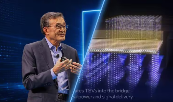
EMIB relies on silicon bridges embedded in the substrate to connect multiple cores laterally. EMIB-T adds TSV (Through Silicon Via) to this architecture, which is a vertical interconnection channel that penetrates the silicon wafer to directly transmit power and signals.
Foveros goes one step further by stacking computing dies or other chips vertically on top of the base die. This structure can reduce the lateral area of the package and shorten the interconnection lines, which is expected to increase bandwidth and improve energy efficiency.
For Nvidia, diversification of back-end packaging suppliers can reduce dependence on TSMC's packaging production capacity - currently there is strong demand for global AI accelerators and TSMC's packaging production capacity is highly tight.
For Intel, if it wins Feynman-related projects, the greater significance lies in completing the industrial verification of Foveros technology rather than achieving immediate victory in the advanced lithography track.
Comments