
Abstract:
Intel's foundry business may usher in another important customer cooperation opportunity. According to the latest forecast by Jeff Pu, an analyst at South Korea's GF Securities, Nvidia may use Intel's Foveros advanced packaging technology in some new-generation AI chips starting in the second half of 2028. This means that even if Intel is temporarily unable to fully challenge TSMC in the most advanced logic process field, it still has the opportunity to enter Nvidia's next-generation chip supply chain with its advanced packaging technology.
This news is not the first to appear. As early as January 2026, there were reports that Nvidia may consider using Intel’s advanced manufacturing technology in a new generation GPU platform code-named Feynman. Relevant news at the time mainly focused on Intel's 18A or 14A process, and whether Nvidia would hand over some non-core chip components to Intel for manufacturing. This time, GF Securities’ forecast further focuses on Foveros packaging technology.
It should be noted that the current relevant information comes from analyst forecasts and does not mean that Nvidia has officially confirmed the adoption of Foveros, nor does it mean that both parties have announced specific orders. Whether NVIDIA will ultimately use Intel technology, as well as which products and how much production capacity will be used, remains to be confirmed by further news.
To understand the significance of this potential collaboration, we first need to distinguish between the front-end process and back-end packaging in chip manufacturing. Front-end manufacturing is mainly responsible for manufacturing transistors and related circuits on silicon wafers, which determines the computing power, power consumption and some performance characteristics of the chip; the back-end is responsible for cutting, interconnecting, packaging and testing the manufactured chips to make them into complete products that can be installed in servers or other equipment.
For modern AI accelerators, back-end packaging is no longer just the last step in the production process, but an important link in determining product performance. As the scale of GPU continues to expand, relying solely on one large chip to complete all computing tasks is facing limitations in manufacturing cost, yield, and design complexity. Therefore, chip manufacturers are increasingly inclined to split different functions into multiple small chips and then integrate them through advanced packaging technology.
Nvidia’s next-generation AI processor is also expected to further adopt this multi-chip design idea. By integrating multiple computing chips, I/O chips, and other functional modules, manufacturers can choose appropriate manufacturing processes based on the characteristics of different components while improving the design flexibility of the overall system.
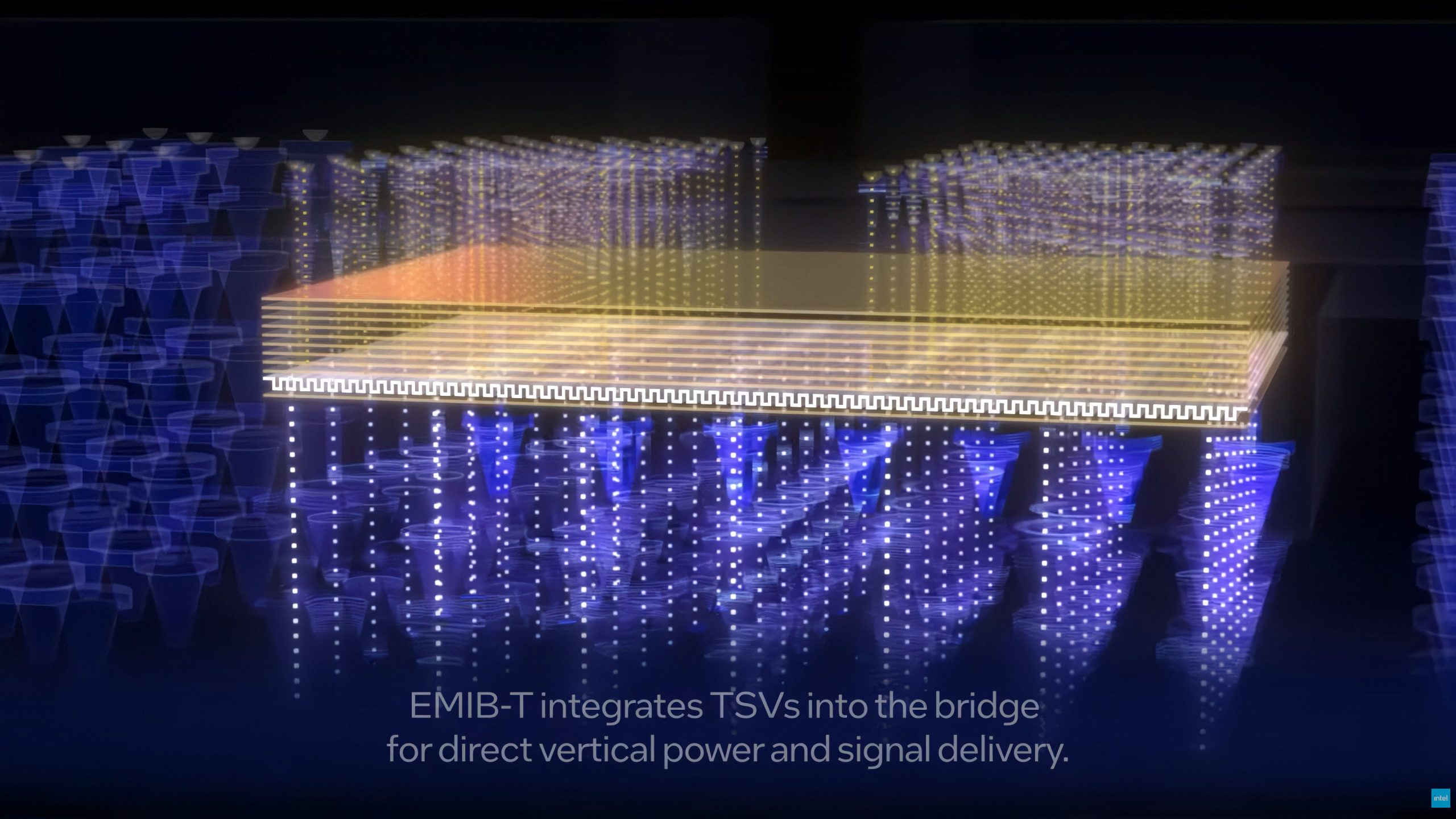
One of Intel's advantages is its continuously developing advanced packaging technology system. Among them, EMIB and Foveros are two representative technologies, but their design ideas are different.
EMIB uses embedded multi-chip interconnect bridge technology to connect adjacent chips by setting up a high-density interconnect structure inside the package. It mainly solves the problem of high-speed communication between multiple chips, allowing different chips to exchange large amounts of data over a short distance.
Foveros goes a step further and can stack different chips vertically instead of just arranging them side by side on the packaging plane. Through vertical stacking, designers can reduce the package's planar footprint and shorten some interconnect paths while meeting design requirements, thereby improving data transmission efficiency and energy consumption performance.
These features are of practical value for AI accelerators that need to process massive amounts of data. As the number of computing chips increases, data transmission between chips may become an important factor limiting overall performance. Advanced packaging can help designers integrate more computing resources in limited space and improve communication efficiency between different components.
However, Foveros is not a single fixed solution, but a packaging technology system that includes different technical routes. Which Foveros solution is used in a specific product will depend on chip structure, interconnect density, power consumption, heat dissipation and manufacturing requirements. Therefore, this rumor cannot be simply understood as Nvidia has determined to use a specific three-dimensional stacking process.
Intel has been working hard to expand its advanced packaging business in recent years, hoping to attract more external customers. For Intel's foundry unit, advanced packaging has special strategic value: even if customers are temporarily unwilling to use Intel's most advanced transistor processes, they may be willing to hand over some chip packaging and interconnection work to Intel.
This model can reduce the difficulty for customers to switch suppliers. For Nvidia, which already produces core GPUs at TSMC, completely replacing the front-end manufacturing process involves a lot of design adaptation, verification and mass production risks, and handing over some back-end packaging links to Intel may become a relatively easy way to try cooperation.
If Nvidia ultimately decides to adopt Intel Foveros technology, both parties will not necessarily need to transfer the entire GPU manufacturing process to Intel. It is entirely possible that Nvidia will continue to use TSMC to produce core computing chips, while using Intel to complete the stacking or packaging of some chips. The integration of components provided by different manufacturers through advanced packaging is an important application direction of modern heterogeneous integration technology.
This is one of the reasons why Intel's advanced packaging business has received attention in recent years. Traditionally, the outside world often measures the competitiveness of wafer foundries through the nanometer-level parameters of advanced processes. However, as chip designs become increasingly complex, the importance of advanced packaging continues to rise. Chip manufacturers not only need to create powerful computing chips, but also connect them in a high-bandwidth, low-power manner.
In this field, TSMC has established a mature advanced packaging technology system such as CoWoS, and serves large customers such as Nvidia with its high production capacity and yield. As the demand for AI accelerators continues to grow, advanced packaging capacity has become one of the key resources for the entire industry.
Market research firm TrendForce pointed out in a report released in September 2026 that although technologies such as Intel EMIB-T are competing with TSMC CoWoS, because CoWoS still has advantages in terms of technology maturity and yield, it is expected to remain the mainstream solution in the advanced packaging field of AI chips by 2028.
This means that even if NVIDIA adopts Intel's Foveros technology in the future, it does not necessarily mean that it will completely abandon TSMC's packaging system. A more realistic situation may be that Nvidia chooses multiple packaging technologies based on the structure, performance requirements and supply of different chips to reduce dependence on a single supply chain.
The existing cooperative relationship between Intel and NVIDIA also provides a basis for further expansion of cooperation between the two parties. In September 2025, Nvidia announced an investment of US$5 billion in Intel and reached a cooperation agreement with Intel to develop multiple generations of joint products. The two parties will use NVIDIA's NVLink interconnect technology to connect Intel's CPUs with NVIDIA's GPUs and launch related products for the data center and personal computing markets.
This cooperation itself does not mean that Nvidia has committed to using Intel's advanced wafer manufacturing process. However, it established the basis for cooperation between the two parties in product design, chip interconnection and system integration, and also made it possible to further explore advanced packaging technologies in the future.
For Intel, packaging orders from Nvidia may have meaning beyond the order amount itself. NVIDIA is one of the world's most important AI chip suppliers. If its products can achieve stable mass production on Intel's advanced packaging production lines, it will help Intel prove the reliability of its technology to other large chip design companies.
More importantly, Intel is still working hard to promote the next-generation 14A process. Advanced process research and development requires huge investments, and to maintain long-term investment, it is necessary to obtain sufficient customer orders and capacity utilization. If Intel can attract large customers in the advanced packaging field and gradually expand these cooperation to front-end manufacturing operations, the business prospects of its foundry unit will have the opportunity to improve.
However, advanced packaging orders do not directly solve all of Intel's manufacturing problems. There are significant differences in technology, equipment, process control and customer validation between front-end wafer manufacturing and back-end packaging. Even if Intel successfully obtains Foveros orders, it still needs to prove that its advanced processes can meet the performance, yield, cost and delivery stability requirements of large customers.
For Nvidia, the potential benefits of adopting Intel technology include increasing supply chain options, easing the pressure on advanced packaging production capacity, and exploring design solutions more suitable for the next generation of multi-chip architecture. The computing scale of AI chips continues to expand, and NVIDIA needs to continuously improve the computing power that can be integrated in a single package while controlling the cost and power consumption of data transmission between chips.
With multiple die stacked vertically, heat dissipation, power supply, and manufacturing yields become more complex. Three-dimensional packaging can shorten some interconnect paths, but it does not mean that all indicators will automatically improve. For high-power AI chips, how to effectively export heat from the stacked structure and how to ensure that each chip remains stable in long-term operation are still engineering issues that must be solved.
Therefore, whether Nvidia ultimately chooses Foveros depends not only on whether Intel can provide sufficient packaging capacity, but also on whether the technology can achieve the required performance, yield, cost and reliability standards in actual products.
From a time perspective, GF Securities analysts predict that relevant cooperation may begin to take effect in the second half of 2028. This time point is roughly consistent with the time when Intel's 14A process plan enters the production stage, and is also related to the product evolution cycle of Nvidia's future generations of AI chips. However, the process launch time is not exactly the same as the mass production time of specific customer products. The latter still needs to go through multiple stages such as design finalization, process verification and production ramp-up.
Overall, this rumor reflects the changes taking place in the AI chip industry chain: advanced manufacturing processes are important, but advanced packaging has become one of the key technologies that determine the performance, cost and supply capabilities of high-end processors. For Intel, securing top customers like Nvidia may become an important opportunity for its advanced packaging business to move forward; for Nvidia, increasing the number of available manufacturing and packaging partners will help cope with the supply chain pressure caused by the continued growth in AI infrastructure demand.
But until Nvidia or Intel officially announce specific cooperation, the adoption of Foveros in the second half of 2028 should still be regarded as an analyst forecast rather than a finalized commercial order. What really determines whether this cooperation can be implemented will be whether Intel can prove in the next two years that its advanced packaging technology has the ability to meet the mass production needs of next-generation AI chips.
Comments