
Abstract:
ASML is working with customers to develop larger masks for next-generation High-NA EUV lithography equipment, an adjustment that is expected to make the system more suitable for the largest AI and data center chips. The company stated that existing EUV equipment can print chips with an area of approximately 800 square millimeters, which is enough to cover processors and accelerators designed for advanced data center hardware by manufacturers such as Nvidia and Google.
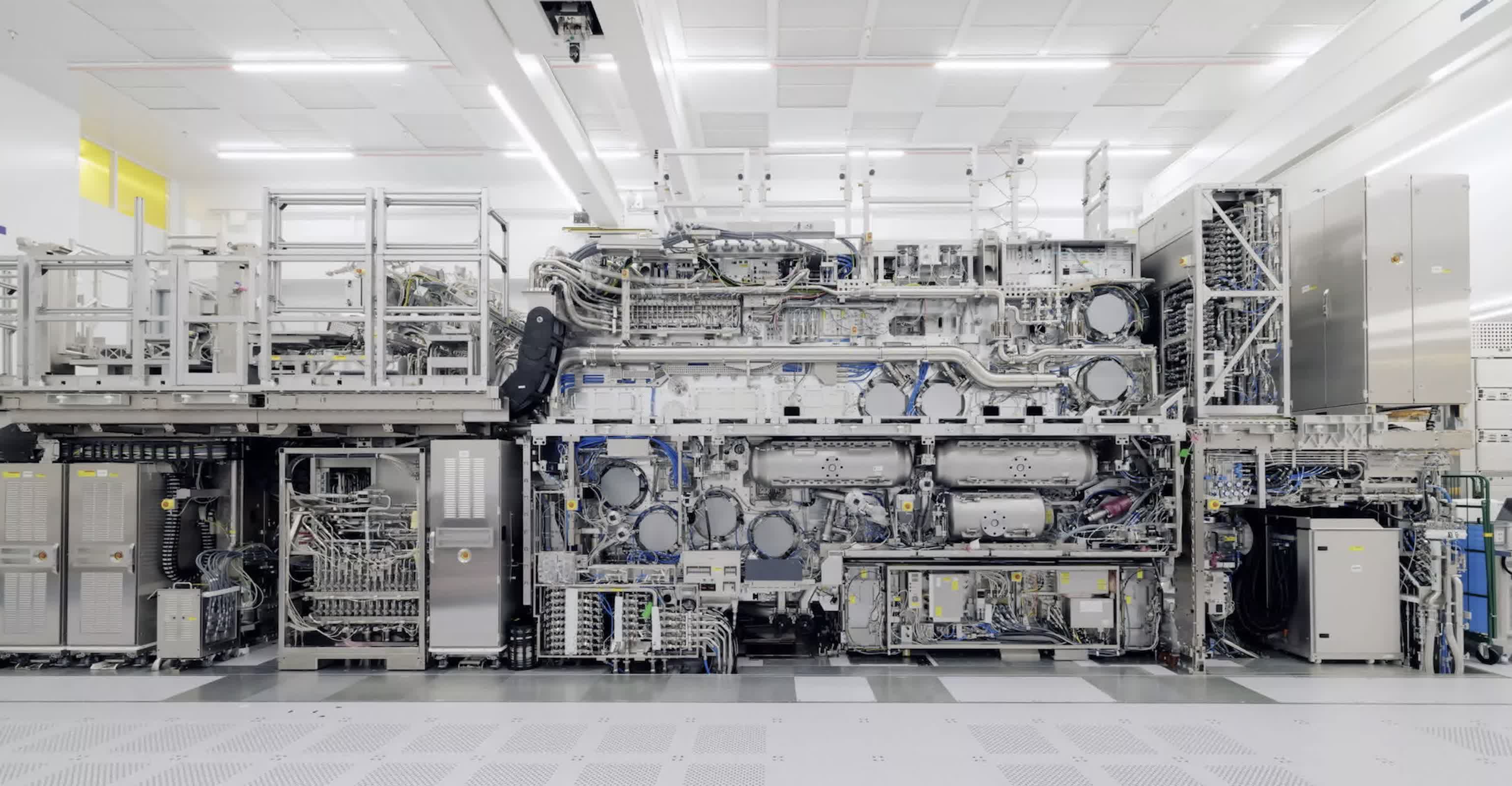
High-NA EUV is ASML's next-generation main lithography platform. It can print finer features than existing EUV, helping chip manufacturers achieve higher-density designs on advanced processes. But it currently uses a smaller mask, which limits the chip area that can be printed in a single exposure.
To address this limitation, ASML plans to move High-NA EUV to a 12-inch reticle format, enabling the new equipment to handle larger chips and cover the largest data center-grade device scale that existing EUV equipment can already produce. Lithography equipment projects circuit patterns onto silicon wafers by letting light pass through a mask that carries chip patterns. Therefore, the size of the mask directly determines how much design content can be covered in one exposure.
In terms of industrial implementation, Intel has used ASML's High-NA system on notebook chips, but TSMC and Samsung have not yet deployed this equipment in large-scale mass production of logic chips. ASML expects to demonstrate a pilot line using a larger mask in 2031 and plans to bring the technology into high-volume production in 2033.
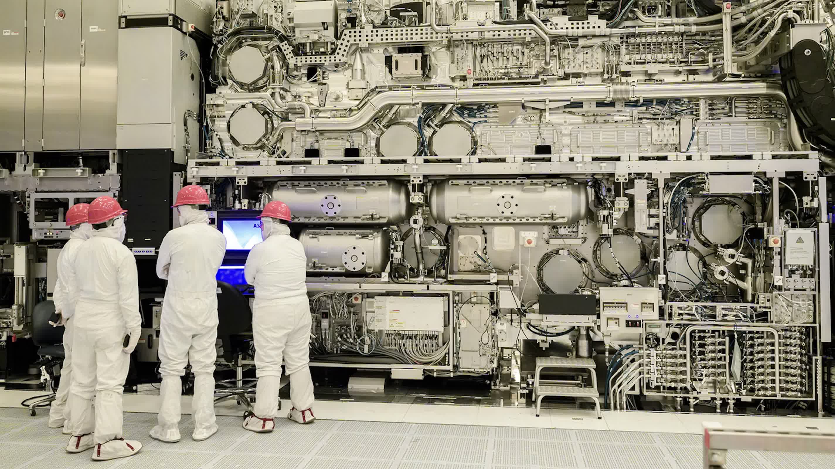
ASML Chief Technology Officer Marco Pieters told Reuters that if all parties in the industry can work together to advance, the production efficiency of these systems is expected to increase by 40%. This move also aims to expand the scope of application of High-NA EUV, because this type of equipment is expected to be more expensive and technically demanding than existing EUV, and chip manufacturers will only be willing to adopt it on a large scale if the output is high enough.
The industry timeline also shows that High-NA EUV is gradually moving from early trials to wider production planning. SK Hynix said it is considering whether to join the alliance to promote the introduction of 12-inch masks, and has set 2028 as the target time point for using High-NA EUV for DRAM mass production; Samsung also plans to use High-NA EUV for high-capacity DRAM production in 2028, and TSMC expects to introduce this technology in the large-scale manufacturing of advanced process chips from 2030.
These developments show that ASML’s large-size mask solution is mainly solving another level of problems: allowing High-NA EUV not only to provide higher resolution, but also to support the increasingly larger chip designs required by AI systems and cloud infrastructure.
Comments