
Abstract:
Intel has made an important step forward in advanced chip manufacturing. On September 8, local time, Intel's wafer foundry department announced that the cumulative processing volume of wafers using high numerical aperture extreme ultraviolet lithography technology has exceeded 1 million. This number covers equipment certification, testing, research and development, and mass production of some product layers, indicating that Intel is gradually advancing this next-generation lithography technology from the laboratory to the actual production environment.
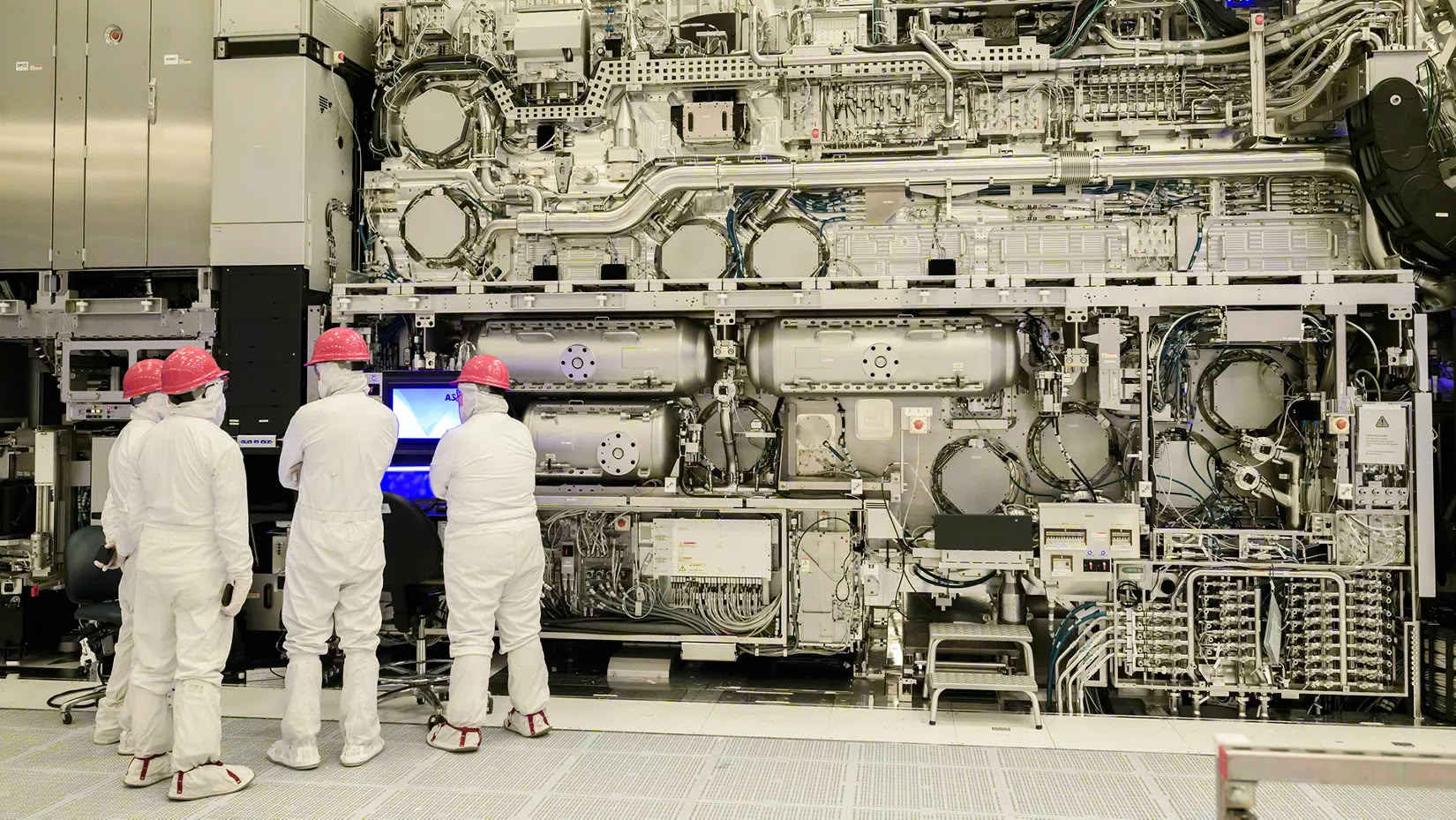
This milestone was announced during the SPIE Photomask Technology and Extreme Ultraviolet Lithography Conference in Monterey, California, USA. Intel said its high numerical aperture EUV wafer processing volume has exceeded the sum of other chip manufacturers using this technology in the world, further consolidating the company's first-mover advantage in this new technology.
High numerical aperture EUV is the next generation version of extreme ultraviolet lithography technology. Its numerical aperture has been increased from 0.33 to 0.55 for traditional EUV equipment. It can form more fine patterns on the wafer and is expected to reduce some complex multiple exposure processes. For advanced processes, this means higher transistor density, lower manufacturing complexity, and the potential to further improve chip performance and energy efficiency. However, the cost and process requirements of this type of equipment are also significantly higher.
Intel has currently deployed at least three high numerical aperture EUV lithography machines in Oregon and uses them for the production of some Intel 18A processes. The company said that the overlay accuracy, production throughput and equipment availability of some Panther Lake processor layers manufactured using this technology have reached expected levels.
It is worth noting that Intel does not hand over the entire 18A process to high numerical aperture EUV, but selects some key layers for production. These layers were verified with both high numerical aperture EUV and conventional 0.33 numerical aperture EUV equipment to compare the manufacturing performance of the two technologies. Intel said that the performance of some 18A layers produced using high numerical aperture EUV has reached or exceeded the corresponding layers manufactured on traditional EUV platforms.
These results also echo Intel’s previously announced Panther Lake processor plans. Panther Lake belongs to the Intel Core Ultra Series 3 series and uses the 18A process. By introducing high numerical aperture EUV in some product layers, Intel can accumulate actual mass production experience without completely relying on new equipment and prepare for more advanced processes in the future.
Intel's wafer foundry department stated that the current high numerical aperture EUV has entered the mass production stage, and the company is continuing to optimize equipment settings, run times and manufacturing processes. Intel and ASML are also working closely to further improve the maturity of this technology and determine the scope of using high numerical aperture EUV in future processes based on customer needs.
In addition to exceeding one million wafer processing volumes, Intel is also promoting the development of larger-size photomasks. Due to the small size of photomasks currently used in high numerical aperture EUV equipment, the chip area that can be exposed at one time is limited. For future data center chips and AI accelerators with larger areas, this may become an important factor affecting production efficiency.
In order to solve this problem, Intel has cooperated with ASML, photomask manufacturers, automation equipment suppliers, EDA software companies, material suppliers, and other chip manufacturers to promote the standardization and supporting infrastructure construction of 6×12-inch large photomasks. The company said that currently customers can already use high numerical aperture EUV through existing 6-inch photomasks, which can not only design chips within the mask range, but also use splicing technology and process design kits to solve larger area manufacturing needs.
Intel believes that future AI products will have increasingly higher requirements for advanced manufacturing technology. Chip manufacturing not only requires higher performance and density, but also stable mass production capabilities and lower adoption thresholds. By promoting high numerical aperture EUV into the production environment in advance, Intel hopes to provide customers with more mature advanced process options.
For Intel, the significance of this progress lies not only in the lithography equipment itself, but also in the fact that the company is gradually establishing mass production experience for high numerical aperture EUV. Compared with traditional EUV, high numerical aperture EUV faces higher requirements in terms of equipment cost, process control, photomask design and production efficiency. Therefore, whoever can complete the transition from R&D to stable production earlier will likely gain greater advantages in future advanced process competition.
However, Intel is still only applying high numerical aperture EUV to part of the 18A layer, which does not mean that all advanced processes have fully adopted this technology. Whether the scope of application can be expanded in the future depends on equipment throughput, production cost, yield, and actual customer needs for the process.
Overall, Intel's high numerical aperture EUV wafer processing volume exceeded 1 million pieces, marking that this next-generation lithography technology is moving from the early verification stage to more mature production applications. As Intel continues to advance its 18A and subsequent 14A processes, high numerical aperture EUV is expected to become an important part of its advanced manufacturing strategy.
Comments