
Abstract:
In Huawei's official definition, Tao's Law is not simply a physical stack of several chips as the outside world mistakenly believes. This is also the biggest misunderstanding of this core technology by the public. Xu Songyu, director of Huawei's Semiconductor Business Wireless Terminal Chip Product Management Department, recently publicly released a technical interpretation.
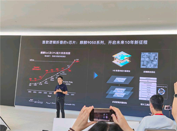
Logical folding technology is by no means a simple physical stacking of multiple chips. Instead, the entire system design is completed from a three-dimensional perspective in the initial stage of chip design, integrating different functions. High-performance logic circuits are distributed in the most suitable position in the three-dimensional space, and multiple DIEs are completely treated as a complete chip for full-link collaborative design, ultimately achieving the effect of shortening signal routing and increasing transistor density, and truly reaping the dual benefits of performance and power consumption.
The Kirin 9050 series, which has been officially launched into mass production, has more than 50 million hybrid bonding points in a single chip and more than 5 million effective signal interconnections. Compared with the previous generation product, the transistor density has been directly increased by 53.5%. Translated into actual use experience, it is an extremely significant improvement in performance and energy efficiency.
Among them, the CPU frequency of Kirin 9050 Pro is increased by 12.7%, the CPU large-core energy efficiency is increased by 41%, the GPU performance is increased by 40%, the GPU energy efficiency is increased by 45%, the NPU computing power is directly increased by 140%, and the NPU energy efficiency is also increased by 66%.
As the core supporting technology of logic folding technology, the process accuracy of hybrid bonding directly determines the final folding effect. Huawei has publicly stated that to achieve effective logic folding, the ratio of the spacing of hybrid bonding to the spacing of the top metal of the chip must be less than 3.
The top metal spacing of Kirin 9050 Pro is 720nm, and the corresponding bonding spacing must be less than 2 microns. Currently, Huawei has achieved the relevant process accuracy to 1.5 microns, and will be able to advance the bonding spacing to 1 micron in 2027. This process will continue to be iteratively optimized.
When the ratio of bonding spacing to top metal spacing reaches 1:1, the critical signal transmission path inside the chip will be greatly shortened, and energy efficiency will reach a new level. At the same time, the reduced spacing can accommodate a larger number of high-speed signal channels, add a large number of interconnection paths, and support the implementation of more complex logic folding designs.
Xu Songyu also specifically revealed that the next-generation Kirin 2027 chip is now ready for development. As of the release of the public interpretation, the test results of all projects are in line with expectations. The logical folding technology route is fully feasible for continuous iterative evolution in the next ten years.
Comments