For a long time, EUV lithography technology has been mainly used to create the most powerful logic and memory chips.However, the Belgian Microelectronics Research Center (IMEC) recently successfully used ASML's EUV lithography equipment for the first time to achieve wafer-level manufacturing of solid-state nanopores on a 300 mm wafer.

This development was hailed by ASML's head of public relations as an "unexpected and outstanding biomedical application."
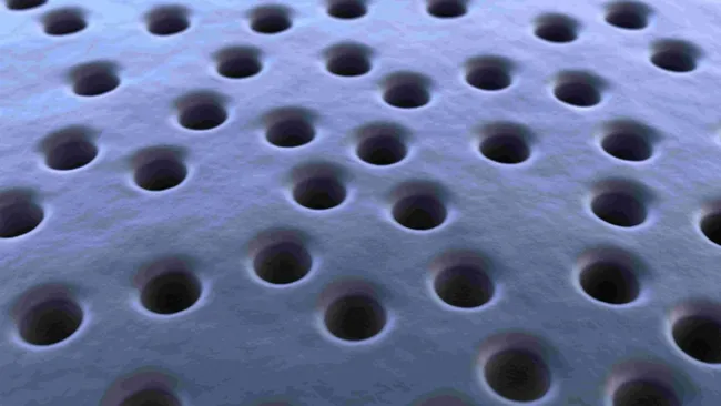
The so-called nanopores are tiny holes with a diameter of only a few nanometers, and their fineness is about one ten thousandth of a human hair. In the field of biosensing, nanopores function like "molecular checkpoints."
When ionic current flows through the hole,The molecules (such as viruses, proteins, or DNA) within them produce unique signals for the electrical current. Based on these unique electrical signals, scientists can identify the size, structure, and charge of the molecules with high sensitivity.
Although nanopores have great potential in genomics and proteomics, large-scale production has not been possible in the past due to manufacturing variability and integration difficulties.
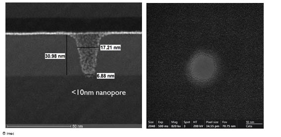
imec's breakthrough is to use EUV technology to ensure a high degree of consistency in pore size. Currently, the pore size has been accurately reduced to about 10 nanometers, and it is expected to break through 5 nanometers through process improvements in the future.
What's more, this method is compatible with CMOS, meaning biosensors can be mass-produced on 300mm wafers just like chips.
imec R&D project manager Ashesh Ray Chaudhuri said applying EUV infrastructure originally used for chip manufacturing to life sciences has opened the door to high-throughput biosensor arrays.