A number of top universities in the United States have cooperated with local wafer factories to successfully develop a new monolithic three-dimensional (3D) chip. The storage and computing units are closely stacked in the vertical direction. It is expected to greatly improve the internal data transmission speed of the chip. It is regarded as an important milestone in breaking through the "memory wall" of artificial intelligence hardware.
This achievement was completed by Stanford University, Carnegie Mellon University, University of Pennsylvania, MIT and SkyWater Technology, a local foundry in the United States. It is the first monolithic 3D chip manufactured in a commercial wafer factory in the United States. Its vertical interconnection wiring density has reached a new high in current 3D chips. The measured and simulated display performance can be improved by about an order of magnitude compared to traditional two-dimensional chips. The research team emphasized that this is not only a breakthrough in performance, but also provides a new paradigm for the United States to promote advanced chip manufacturing locally.
Unlike traditional two-dimensional chips that "tile" all circuits on the same plane, this prototype chip uses multiple layers of ultra-thin circuit layers to be stacked vertically. Each layer is closely connected through high-density vertical connections, so that data can "shuttle up and down" between the storage unit and the computing unit inside the chip, significantly shortening the transmission path. Under such an architecture, the local available memory is significantly increased, and data does not need to frequently travel between remote storage and computing cores, which fundamentally alleviates the "memory wall" bottleneck that has long plagued high-performance and AI chips.
The "memory wall" refers to the continuous improvement of computing power of computing units, but the data transfer rate between the internal chip and external storage is difficult to keep up, causing the processor to often "wait for data" and computing power to be severely wasted. For decades, the semiconductor industry has mainly relied on continuously shrinking the size of transistors and packing more devices on the same plane to alleviate this problem. However, this route is approaching physical limits and is known as the "shrink wall." This new monolithic 3D chip integrates storage and logic circuits in the vertical direction, which is equivalent to building rows of "elevator shafts" inside the chip, allowing a large amount of data to flow between different "floors" at high speed at the same time, thus finding a new way out under the dual constraints of the "memory wall" and the "miniature wall".
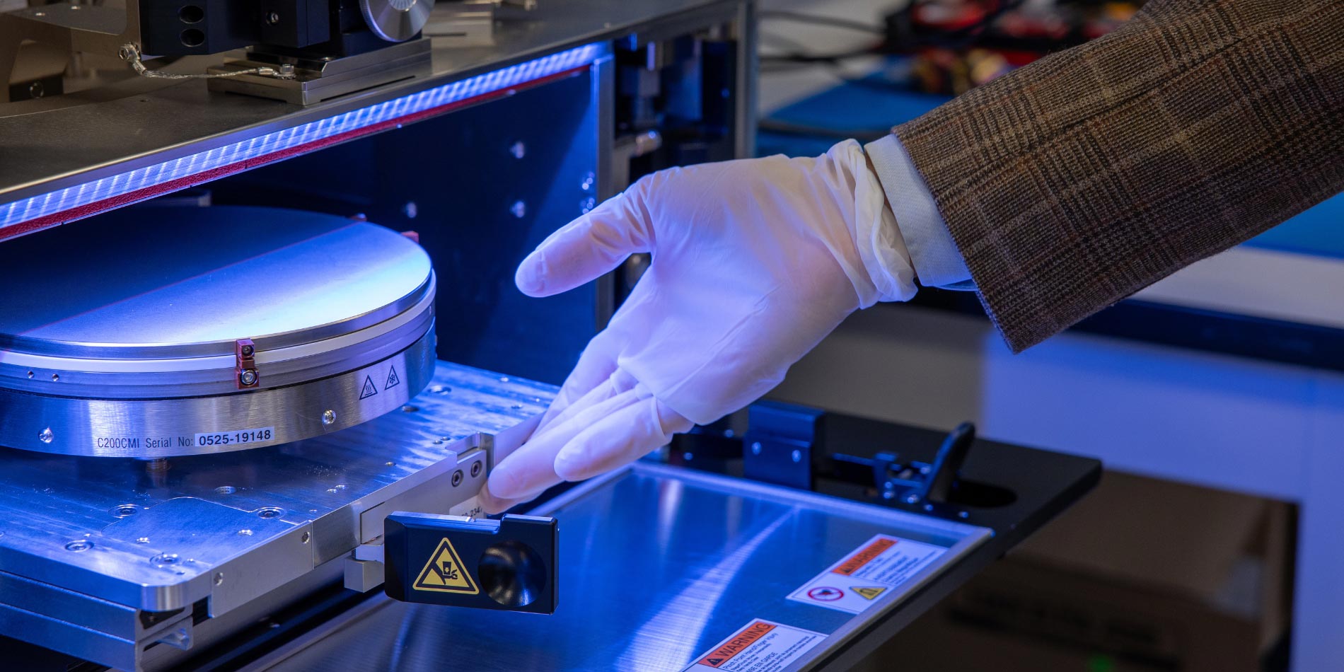
The industry has previously tried to build a 3D system by stacking multiple manufactured chips up and down. However, this "stacked chip" method is often rough and sparse in the inter-layer connections, and there are still obvious bottlenecks. This research uses a "monolithic" 3D process: each functional layer is grown and processed directly on the same wafer in sequence. The low-temperature process avoids damage to the underlying circuits, so high-density interconnection can be performed on a smaller scale. The process, completed entirely at SkyWater's commercial wafer fab in Bloomington, Minn., is seen as an important step from a laboratory concept to a scalable production architecture.
In terms of performance, early hardware testing shows that the current prototype chip has achieved about four times the performance improvement compared to a comparable two-dimensional design. Further simulation results show that when the number of vertical stacking layers is continued to be increased and a higher "floor" architecture is built on this basis, the overall performance can be improved by up to about twelve times on actual AI loads including the Meta open source large model LLaMA. The research team particularly emphasized that the new architecture is theoretically expected to achieve a 100 to 1,000-fold improvement in energy-delay product (EDP), a key indicator that measures the overall performance of speed and energy efficiency.
By greatly shortening the data transfer distance and increasing the number of vertical channels, the chip is expected to achieve both higher throughput and lower energy consumption per operation, eliminating the need to make the traditional "choose one" between performance and power consumption. Researchers regard this as one of the key paths to support the next generation of large-scale AI systems and move towards the goal of “thousand-fold hardware performance improvement”. They believe that this breakthrough opens up a new technical dimension for future AI hardware evolution, with the ability to support training and running larger, more complex, and more real-time models.
The importance of this work is also reflected in the level of industry and talent training: by successfully tape-out of a single 3D chip in a local commercial wafer factory in the United States, the team believes that it has provided a realistic model for building an advanced chip system that is "designed in the United States and manufactured in the United States." Researchers liken it to the integrated circuit revolution of the 1980s - a group of students studying chip design and manufacturing in American universities drove the take-off of the silicon industry. Today's shift to monolithic 3D integration also requires a new generation of engineers to master new process and architecture knowledge.
With funding and collaboration from projects such as the U.S. Microelectronics Commons program and the California-Pacific Northwest AI Hardware Hub (Northwest-AI-Hub), relevant universities have begun to carry out systematic training around 3D integration and AI-specific hardware. Participants pointed out that being able to manufacture advanced 3D chips locally not only means leading in performance indicators, but also means taking greater initiative in the pace of innovation, supply chain security, and the development direction of AI technology.
According to reports, the research was conducted jointly at Stanford University's School of Engineering, Carnegie Mellon University's School of Engineering, the University of Pennsylvania's School of Engineering and Applied Science, and the Massachusetts Institute of Technology, with all chip manufacturing being handled by SkyWater Technology. The project has received funding from the U.S. Defense Advanced Research Projects Agency (DARPA), the U.S. National Science Foundation Graduate Scholarship Program, Samsung, the Stanford Precourt Institute for Energy Research, the Stanford SystemX Alliance, the U.S. Department of Defense’s “Microelectronics Commons” AI Hardware Hub, the U.S. Department of Energy, and the National Science Foundation’s “Semiconductor Future Initiative.”
Compiled from /ScitechDaily