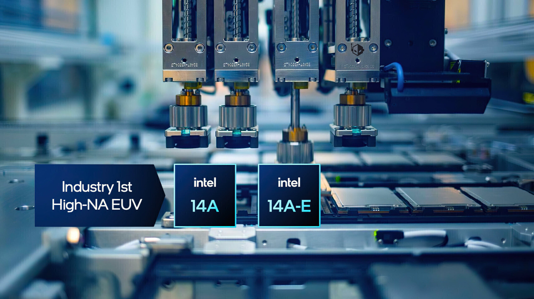
According to a UBS research report, Intel Foundry has recently received great attention in the industry. Many leading global technology companies are expected to announce new foundry cooperation commitments this fall. Intel is considered to be on the verge of winning a number of important new contracts. UBS pointed to Intel’s recent release of version 1.0 process design kit (PDK) for the 14A process node as a key catalyst in pushing these potential orders into the decision-making stage.
In the past period of time, there have been reports in the market that Apple, AMD, Nvidia, Google and Broadcom are considering using Intel's wafer manufacturing capabilities, including advanced process nodes such as 18A, 18A-P, 18A-PT, and the subsequent 14A node. Rumors indicate that Apple is expected to transfer some of its M-series "Apple Silicon" notebook processors to Intel's 18A-P node for production in 2027; Google may use advanced packaging technologies such as Intel's EMIB and Foveros 3D in some TPU (tensor processor) products.
At present, when major chip design companies evaluate leading processes, they usually still give priority to TSMC because of its mature yield rate and large-scale production capacity, as well as its fully proven advanced packaging capabilities in high-performance, low-power designs. However, Intel has continued to increase its capital and supply chain investment in foundry business in recent years, and actively strives to win external customers. This is also the background why UBS expects to see multiple foundry commitment announcements this fall. At the end of last year, there was news that Apple was waiting to see the release progress of Intel 18A-P PDK 1.0 and 1.1 versions, which were planned to be released in the first and second quarters of 2026 respectively. Now that it has entered the second quarter, the outside world is waiting for more signs to confirm whether Apple has finally finalized the cooperation, and UBS tends to believe that Apple has chosen to continue to move forward.
In addition to wafer manufacturing itself, Intel is also regarded as an important breakthrough in the field of advanced packaging. Through EMIB, and its extended versions EMIB-T and EMIB-M, customers can integrate multiple chiplets and multiple HBM high-bandwidth memories into a single package based on 2D, 2.5D and 3D forms. Intel has demonstrated a solution to integrate up to 47 chiplets in a single package and has proposed long-term ideas for multi-kilowatt power packaging solutions. In contrast, CoWoS, TSMC's current main advanced packaging technology, is said to face certain challenges when processing four large mask-sized chips, which has also brought pressure and potential capacity bottlenecks to the mass production of some of Nvidia's high-end products.
In an environment where the United States and its allies hope to reshape the domestic semiconductor supply chain, if Intel Foundry can obtain more orders from large customers in both advanced processes and advanced packaging, it will significantly consolidate its position in the global foundry landscape and bring more supply source options to areas such as high-end computing, AI acceleration, and high-bandwidth packaging.