Applied Materials announced that it has reached an innovative partnership with its long-term partner TSMC to jointly develop key semiconductor technologies for the new generation of artificial intelligence era at its EPIC (Equipment and Process Innovation and Collaboration) center in Silicon Valley, USA, with a total investment of up to US$5 billion. The two parties will carry out collaborative research and development in this center around materials engineering, equipment innovation and process integration, with the goal of achieving more energy-efficient chip performance across the entire link from cloud data centers to terminal devices.
Gary Dickerson, President and CEO of Applied Materials, said that the company and TSMC have had more than 30 years of in-depth cooperation at the forefront of advanced semiconductor technology. This "innovation on the same site" at the EPIC Center will help both parties cope with the unprecedented complexity of the process roadmap faster and accelerate the advancement of breakthrough technologies from early-stage research to large-scale mass production. Wei Zhejia, executive vice president and co-chief operating officer of TSMC, pointed out that as each generation of semiconductor device architecture continues to evolve, the difficulty of material engineering and process integration continues to rise. To meet the explosive demand for AI computing power on a global scale, closer collaboration within the industry chain is required. He emphasized that the EPIC Center provides an ideal environment to accelerate the maturity of new generation equipment and processes.
According to the two parties, through the cooperation of the EPIC Center, Applied Materials and TSMC will focus on a series of key challenges faced by current advanced logic processes as they continue to "shrink, stack and improve efficiency." Key directions include: first, developing new process technologies that can continuously improve power consumption, performance and area (PPA) on leading process nodes to support the higher requirements of AI and high-performance computing on chips; second, introducing new materials and new generation manufacturing equipment to achieve precise construction of complex 3D transistors and interconnect structures; third, improving yield, process fluctuation control and reliability through advanced process integration solutions, laying the foundation for the evolution to vertical stacking and extreme scaling architectures.
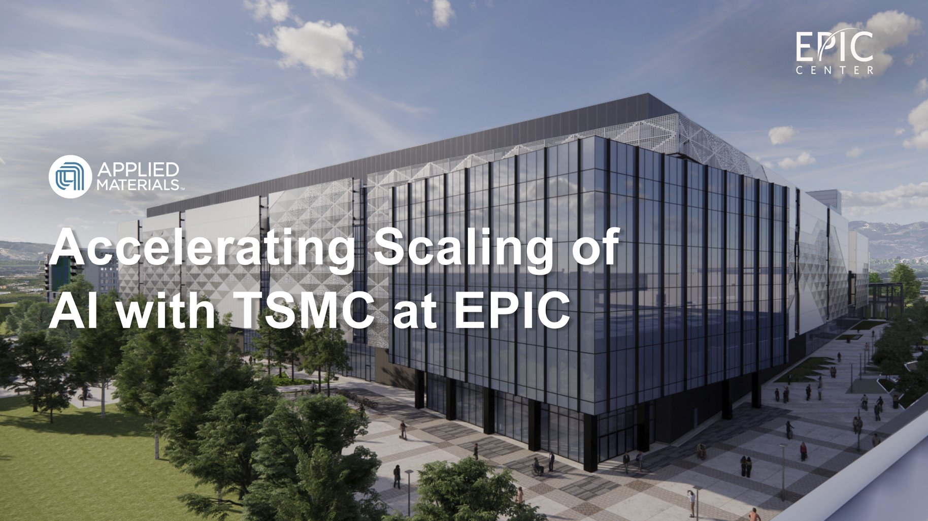
The EPIC Center is known as the largest single investment in advanced semiconductor equipment research and development in the United States to date. The overall plan aims to significantly shorten the technology transformation cycle from laboratory to mass production factory. The center is expected to be operational this year, and its facilities have been optimized from the beginning for the goal of "rapidly moving from early R&D to mass production verification." For wafer fab customers, including TSMC, the EPIC Center will provide earlier access to the Applied Materials R&D portfolio, accelerate test iterations, and accelerate the introduction of next-generation technologies into high-capacity production lines in a safe and controllable collaborative environment.
Applied Materials said that through the co-creation model of the EPIC Center, the company can not only bring higher R&D efficiency and value sharing to partners, but also gain a forward-looking perspective of longer cycles and multiple process nodes to more targeted layout of internal R&D resources. Driven by AI, the trend of chips evolving towards complex 3D devices and interconnect structures has become increasingly clear. The industry generally believes that how to cross the technical threshold known as the "3D transistor wall" will largely determine the upper limit of AI chip performance and energy efficiency in the next stage. The cooperation between Applied Materials and TSMC in the EPIC Center is regarded as one of the important layouts of the industry chain in this direction.