In 2026, a law named by a Chinese company is causing a "tremendous shock" in the global semiconductor industry. While the Western industry is still debating whether Moore's Law has come to an end, He Tingbo, director of Huawei Technologies Co., Ltd. and president of the Semiconductor Business Unit, released a new direction of technological evolution at the International Circuit Systems Symposium (ISCAS 2026) - "Tao (τ) Law."
In the chip industry, the core logic of the evolution of traditional chip technology is to make transistors smaller and smaller, but this path is approaching the dual limits of physics and economics. The law announced by Huawei this time is to shift the focus of chip development from traditional "geometric space shrinkage" (making transistors smaller) to "time shrinkage" (shortening signal transmission time). Through technologies such as logic folding, semiconductors and electronic systems will continue to evolve.
In the past six years, Huawei has designed and mass-produced 381 chips based on this idea. This fall, the first Kirin chip that fully adopts logic folding technology will be available. Huawei predicts that by 2031, the transistor density of high-end chips based on Tao (τ) law will reach the same level as the 1.4nm process.
But a more acute question is also facing the industry: Is Tao (τ) Law a real "new law", or is it self-help marketing under limited technology?
"The key point is not whether Tao (τ) Law has really become a new 'law' on the level of Moore's Law." An industry analyst said that the more important signal of Tao (τ) Law than replacing Moore is that it breaks the shackles of "process-only theory" for the first time and opens up another possible development path for the industry, although it is still full of challenges.
An alternative to Moore's Law?
For more than half a century, Moore's Law has driven the progress of the semiconductor industry. At its core is geometric scaling: every 18 to 24 months, transistor density doubles, performance increases, and costs fall. But in today's semiconductor industry, it is increasingly difficult to continue to rely on size reduction in exchange for performance improvements.
On May 25, He Tingbo mentioned in a signed paper "Time Shrinkage Theory of Multilayer Electronic Systems" that for most of history, the semiconductor industry had only one thing to do: make transistors smaller, but after 7nm, the returns from pure size shrinkage have flattened. Mask costs, EUV depreciation and design rule complexity have pushed leading-edge chip design budgets at the 2nm node to over a billion dollars.
The core essence of the "Tao (τ) Law" proposed by Huawei is that it no longer relies on the reduction of geometric size, but is realized by compressing the effective constant τ at various levels such as devices, circuits, chips, and systems.
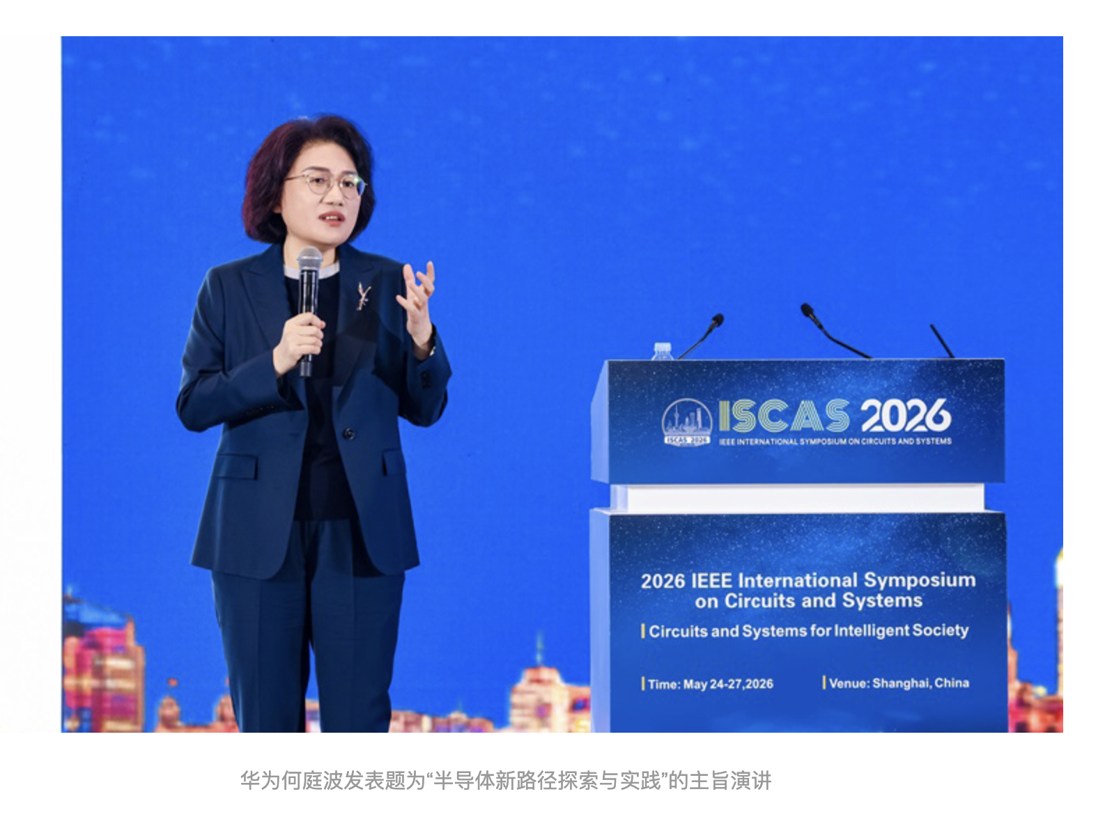
"The common job of all chips is to transport data. The previous optimization of the geometric scale was mainly to use better lithography machines to print higher-density electronic paths to speed up. But now the width of the electronic paths is almost the same as the car running on it, so there will be leakage and data loss. In fact, Moore's Law has encountered a bottleneck. "A Huawei insider told reporters that optimization on the time scale, for example, the propagation speed of electrical signals on the chip medium is only 50% of its speed in vacuum, but as long as there is a breakthrough in materials science and the material has a better dielectric coefficient, there is room for improvement.
But Huawei is not the first company to seek alternatives in the post-Moore era. Previously, NVIDIA had also increased investment in system integration, including NVLink, NVSwitch, CoWoS packaging, HBM integration, software ecosystem, and rack-level architecture. AMD pursues small chips (chiplets) and advanced packaging technologies. Intel's Foveros and TSMC's SoIC also represent their respective efforts in vertical integration and three-dimensional stacking. The success of Apple's M-series chips is largely due to the localization of memory and the vertical integration of hardware and software.
"Semiconductor companies such as TSMC are already doing 3D stacking, hybrid bonding, optical replacement of copper, etc." Hu Yanping, a distinguished professor at Shanghai University of Finance and Economics, said in a signed article that questions during the industry discussion mainly focus on three points: The first point, "Tao "(τ) Law" is a distinctive new path, or is it actually a path that everyone will take; second point, is this a path of gradual, optimized, and improved, or is it a brand-new system; third point, is this a lane change to overtake, or more basic difficulties need to be overcome.
He believes that although there have been mathematical calculations, "Tao (τ)'s Law" is not yet a development law in the semiconductor field in the strict sense. It is only a calculation theory refined based on practice, as well as a system judgment and development expectation for the future. It cannot be compared with Moore's Law in a short time. However, from the perspective of process delays, changing computing architecture, and the formation of a new space-time view of computing systems, it is not impossible for "Tao (τ)'s Law" to become a law.
"There are no eternal laws in the manufacturing process. It will be good if it can continue to be effective for more than ten years. At present, the demand for AI computing power continues to explode. The demand for computing is not only to increase transistor density and improve energy efficiency ratio, but also to accelerate the evolution of the future architecture of SICAS." Hu Yanping said that the semiconductor industry is indeed at an important turning point in the development process. At this turning point, someone must send a turning signal and companies must make turning moves. The industry is moving forward in different directions such as von Neumann architecture, ternary system, brain-inspired computing, optical computing, and quantum computing. Companies, including Huawei, will not stay in path dependence.
In the paper submitted by He Tingbo, it is mentioned that a considerable part of the gains in speed performance of the chip are not obtained through new photolithography process steps, but through topological reorganization of logical distribution in three-dimensional space, and this direction is sustainable. This method is like "upgrading a bungalow to a skyscraper." The traditional chip design is 2D planar, and the signal travels between tens of billions of "threshold switches" (transistors). However, in a skyscraper, signals that originally required long-distance horizontal transmission can now be "taken in an elevator" to travel vertically, and the physical distance is drastically shortened.
This is fundamentally different from Moore's Law, because the power of driving technology is no longer the pursuit of process and the breakthrough of a single lithography node, but relies on the systematization of the four levels of devices, circuits, chips, and systems. It is this multi-dimensional fundamental change that forces the semiconductor industry to re-examine its future evolution direction.
What is the impact on the industry?
When the rules of the game changed from "geometric space" to "time system", the players at the card table also began to worry about whether they would face a cruel shuffle. In interviews, some people told reporters that there are opportunities and challenges.
For the industry, under Tao's (τ) law, areas that were previously regarded as "supporting roles" such as packaging technology, new materials, interconnection architecture, and system software collaborative design have gradually assumed a key position. If any company can achieve innovation in system-level design, such as effectively compressing the τ value through advanced 3D stacking and inter-chip interconnect protocols, it is possible to surpass opponents in performance that use more advanced but costly processes.
This undoubtedly opens a new window of opportunity for companies with strong system integration capabilities, as well as many domestic start-up chiplet and advanced packaging companies.
"The inability to obtain the most advanced EUV and leading foundry services has relieved Huawei of its burden. Facts have proven that intergenerational performance improvements can also be achieved through system-level time optimization without relying on the most advanced nodes. This directly challenges the cornerstone of the former's competitive advantage. "A senior person in the semiconductor industry told reporters that the organizational structure, talent reserve, technology accumulation and capital allocation of companies that rely on Moore's Law are all centered around "process nodes". What they are good at is "making a function the best", while τ Law requires full-stack capabilities.
In his speech, He Tingbo also repeatedly emphasized collaborative optimization from devices to systems. Huawei's "Unified Bus (UB)", "HiONE Optical Interconnect Engine", "System Folding", etc. are all system-level projects.
However, some industry chain companies have expressed concerns. A person in charge of semiconductor upstream equipment told reporters: At present, this theory has limited impact on the industry in the short term, but if the subsequent technology path is advanced to processes below 1 nanometer, the industry will face severe challenges.
"Huawei's technical solution relies on soft technologies such as architecture and algorithms to achieve performance equivalence in the absence of top lithography machines. However, this model cannot replace technical challenges at the hardware level." The above-mentioned person said that the development situation of domestic and foreign chip companies is significantly different. Overseas manufacturers can leverage advanced process resources such as TSMC and Samsung. Domestic companies have greater resistance to development, and industry development still relies on simultaneous technological breakthroughs in the software and hardware fields.
In addition, from the time a theory is proposed to becoming an industry consensus, it is bound to be accompanied by huge risks and practical challenges. Moore's Law is successful not only because of improvements in transistor density, but also because these improvements are accompanied by economically scalable manufacturing processes. The τ law is currently more like an excellent system engineering principle, but it has not yet been proven to be a general and universal economic law. When it is necessary to mass-produce millions or even tens of millions of chips and withstand the cost pressure of the consumer market, it is still a huge unknown whether τ's microscopic economic accounts can be calculated.
"Tao's (τ) law means that the degree of difficulty is greater to a certain extent." Hu Yanping said that fundamental challenges such as equipment, process, technology, yield and even heat dissipation and EDA coexist with self-challenges. This law is not an official announcement of being far ahead, but a fusion and refinement of playing styles, a brave expectation for the future, and a comprehensive innovation of the system.
However, in his view, advanced processes are becoming "not the only one" and the process itself is slowing down, giving domestic chips and new computing systems room for innovation from a time perspective.
Although the road ahead is long and full of thorns, Huawei is also using its own case to illustrate the feasibility of this law. He Tingbo gave a set of data in the paper. From May 2020 to May 2026, Huawei Semiconductor designed and mass-produced 381 chips to serve the mobile, AI, automotive, industrial and infrastructure markets. Across the entire product portfolio, the τ microfilm thesis holds up. In 2029, CPU performance core frequency is expected to move towards 4GHz and above, Kirin SoC efficiency is expected to more than double under typical use within three to five years, and AI hardware integration is expected to increase by more than 100 times by 2035.
She said that the "Tao (τ) law" is showing industry strategists and capital allocators that the next investment should follow τ rather than nodes. Product competitiveness no longer relies entirely on top-notch photolithography processes. The strategic positions of chip packaging, memory bandwidth, and interconnect architecture have become comparable to the advanced logic processes of the past.
It's a difficult transition for a generation of engineers who grew up equating "Moore's Law" with "progress." "The era of geometry is actually over, and denying this fact is not a feasible strategy. The era of acceleration through microscale is giving way to the era of acceleration through τ optimization of multi-layer electronic systems." He Tingbo said.
At the end of her paper, she issued a call to the industry and said that in the next six to ten years, enterprises, scientific research teams and industrial ecology with τ as their core research and development goals will dominate the development pattern of the computing industry in the following ten years.
"The technology development framework for the next ten years has been clear, but there are still many unsolved problems that cannot be overcome by a single company. Tool chains, industry standards, performance benchmarks, device physics, business models and other fields require collaborative creation by the entire industry." He Tingbo said.