
Abstract:
NVIDIA recently announced NVHBM (NVIDIA High Bandwidth Memory) custom high-bandwidth memory technology. Unlike traditional HBM solutions that integrate memory controllers on computing chips, NVHBM sinks related functions into the base die of the 3D HBM stack. Nvidia plans to adopt the technology in future GPUs and expand it to third-party XPU customers through NVLink Fusion.
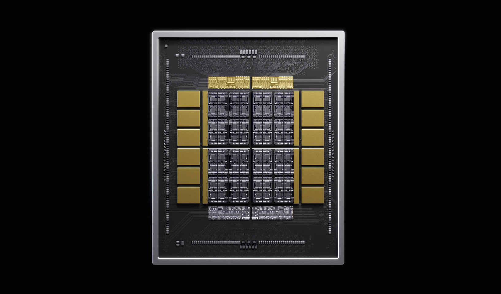
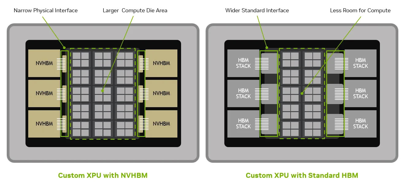
Traditional HBM architecture usually deploys memory controllers on the computing die, thus occupying valuable silicon area that could otherwise be used for computing units. NVHBM aims to simultaneously improve bandwidth, energy efficiency, and the available area of the computing die by moving the controller inside the HBM stack. According to data given by NVIDIA, compared with standard HBM4E, NVHBM can achieve up to 30% increase in memory bandwidth, 15% reduction in HBM power consumption, and allow the processor computing die to obtain up to 25% additional available area.
The area savings mainly come from the redesigned physical memory interface. Standard HBM uses wider interface connections, which will expand the packaging space; NVHBM’s customized PHY can reduce the I/O area by up to 67% compared to JEDEC HBM4E. Narrower interfaces also simplify interposer routing, freeing up to 80% additional available silicon space in the overall layout. NVIDIA points out that the reduced PHY footprint means reduced routing constraints on the interposer, which is especially important for integrating multiple sets of HBM stacks next to large computing dies.
In terms of energy consumption, the 15% reduction in HBM power consumption is not only significant in improving efficiency, but also releases more heat dissipation margin for computing die. This advantage is especially critical for enterprise-scale deployments and data centers: when thousands of compute units are running simultaneously in hundreds of racks, energy efficiency improvements in individual components are significantly amplified. NVIDIA takes a data center with a 2000W XPU and a total power scale of 1GW as an example. The saved power margin can theoretically support the deployment of up to 15,000 additional XPUs.
It is worth mentioning that Samsung recently launched a new product in Hot Chips It was confirmed at the 2026 conference that HBM4E is preparing to ship a single-pin rate of 16Gbps, which is a further improvement compared to the current 14Gbps version. The existing 14Gbps HBM4E provides 3.6TB/s of bandwidth per stack through 2048 pins, while the 16Gbps version can increase this value to 4TB/s. If the 30% bandwidth increase claimed by Nvidia is added to this, the theoretical bandwidth of a single group of NVHBM is expected to reach approximately 5.2TB/s.
NVIDIA stated that NVHBM will accept verification from multiple memory suppliers to simplify the supplier certification process for customers. Annapurna Labs, a subsidiary of Amazon, has become the first partner to confirm that it will cooperate with NVIDIA to promote NVHBM.
Comments