
Abstract:
在Hot Chips大会上,英特尔公布了18A-P制程工艺的更多细节。这一工艺引入了环绕式栅极(GAA)晶体管、背面供电(GAA-BSPD)、Power Boost技术,并增加了金属层数,在低电压条件下可为x86"量产"硅片带来高达30%的运行频率提升。
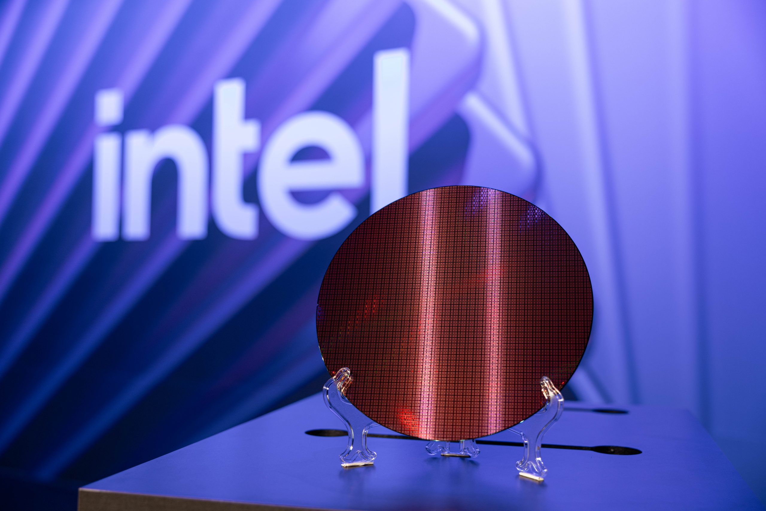
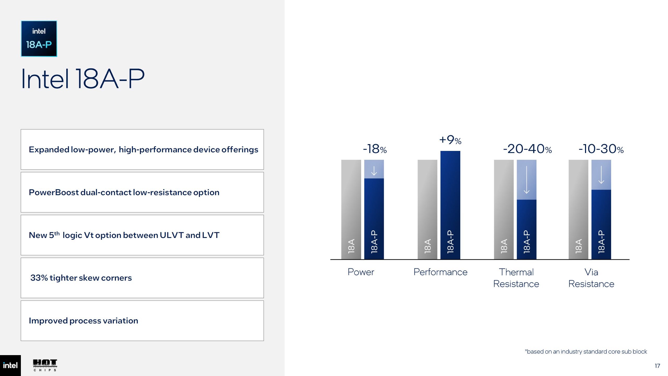
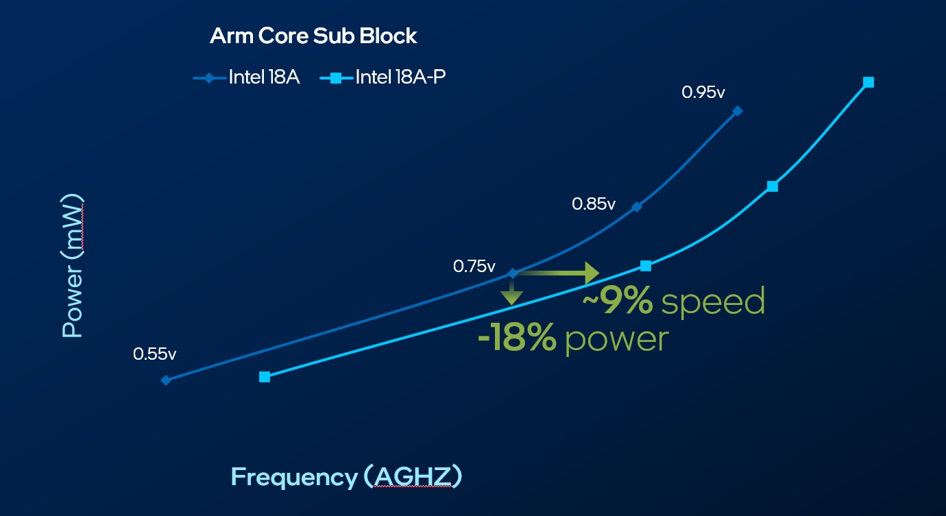
Futurum Research Group与英特尔合作披露了18A-P工艺的具体优势,研究显示该工艺并非18A的简单迭代,而是"刻意"设计用于在低电压下提升能效、在高电压下提升性能。与18A相比,英特尔18A-P在同等功耗下性能提升超过9%,或在同等性能下功耗降低超过18%;该工艺还引入了先进应变工程以增强载流子迁移率,并扩展了RibbonFET产品线,新增了面向AI、移动及数据中心应用的Power Boost技术。
报告中写道:"这些创新技术有望为多代产品的单核性能领先奠定基础。FinFET技术的成熟历经了四代器件与设计协同优化的积累。而带有背面供电的GAA技术目前正处于这一发展曲线的第一步——在量产硅片上已实测到低电压下30%的提升,高电压下也达到两位数增幅。Diamond Rapids与Nova Lake将率先享受到18A-P带来的红利,而钌互连与堆叠逻辑等技术仍在后续规划之中。"
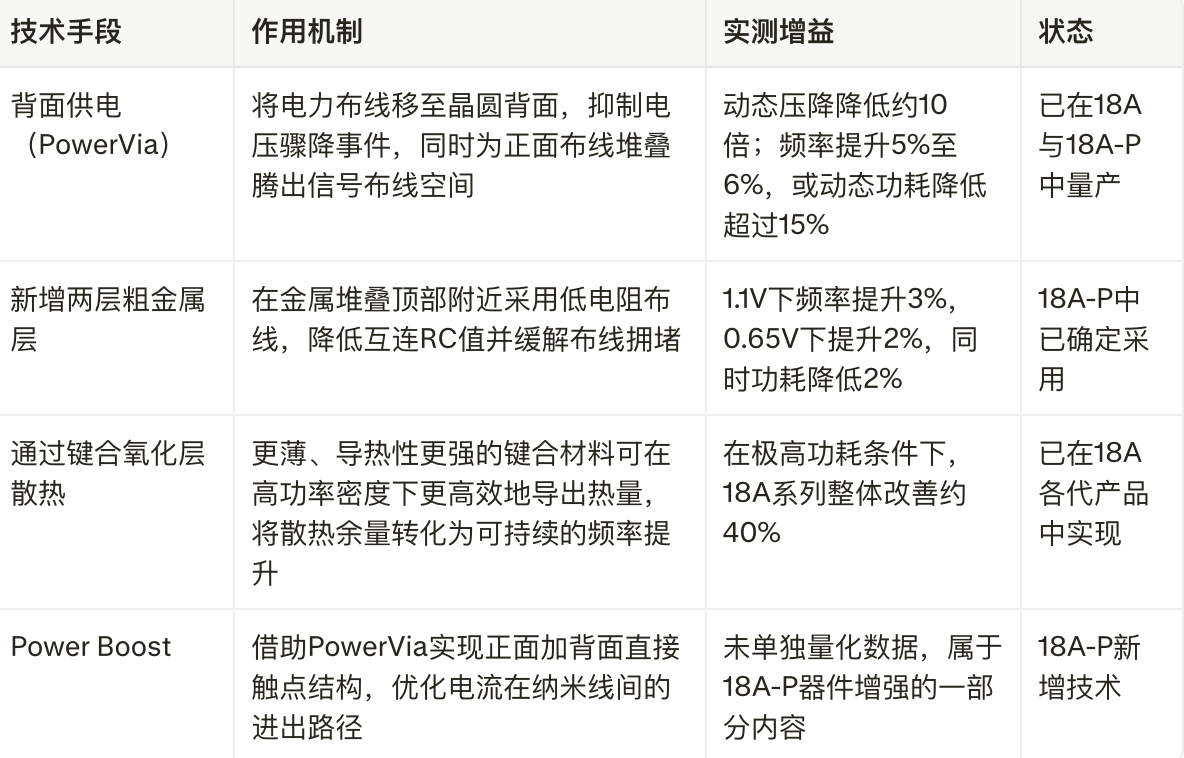
GAA transistor technology is designed to benefit the most in the low-voltage range. At the high-voltage end, backside power supply technologies such as Intel's PowerVia have shown their potential by guiding power from the backside of the wafer instead of the front wiring layer. The study pointed out that the 30% figure comes from direct measurement results, that is, the comparison between the CPU core manufactured based on the GAA back-side power supply process and the FinFET core of the same level over the entire operating voltage range: at 0.5V voltage, the core operating frequency is increased by 30%. This comparison is conducted at the same voltage and core level, so that the impact of architectural changes can be eliminated and the contribution of the process technology itself can be measured separately.
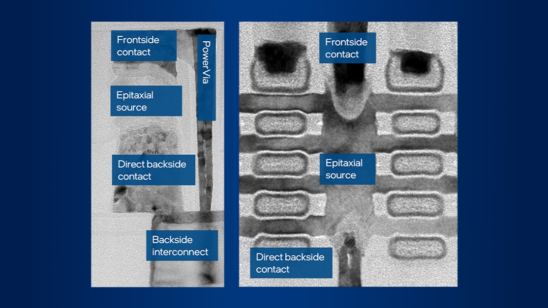
RibbonFET的栅极从四面包裹晶体管通道,使英特尔能够更精确地控制更低的阈值电压。此外,将供电布线移至晶圆背面可减少IR压降,从而降低电压损耗。英特尔研究员Eric Fetzer表示:"背面供电这一概念本质上是对高电压供电的一种改进。它在低电压下也有帮助,但在高电压时会出现较大的压降事件,此时背面供电在降低供电损耗方面效果非常显著……将背面供电与环绕式栅极结合并非偶然,这是把两项互补的技术结合在一起,因此我们同时具备了高电压和低电压两方面的优势故事。"
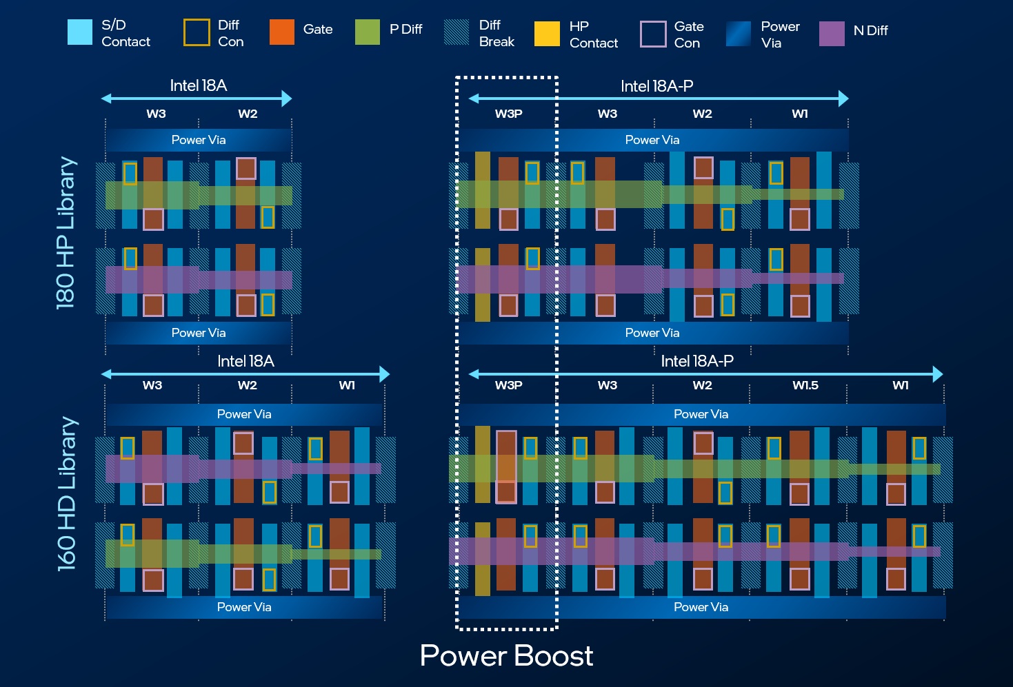
On the 18A process, Intel has demonstrated the effect of back-side power supply converting device gain into core frequency improvement, achieving a 5% frequency increase at 1.1V and a 7.5% frequency increase at 0.95V. In addition, the 18A-P process has expanded the RibbonFET product line, adding device options optimized for different design goals, such as W1 and W1.5 for low-power, low-capacitance devices, and W3P for high-performance applications equipped with Power Boost technology, which can achieve a 10% increase in operating speed without increasing electrical load. Compared with 18A, 18A-P also reduces the external resistance of NMOS devices by 20% and PMOS devices by 12%, while achieving higher current and higher frequency under matching capacitance conditions.
Based on the thermal management innovation introduced in 18A, 18A-P further improves heat dissipation capabilities through material improvements and advanced EDA-driven heat dissipation solutions. 18A-P increases the thermal conductivity of the bonded stack by 50%, improving the thermal resistance of the overall stack by 20% to 40%.
In addition, Intel is evaluating advanced materials and packaging technologies to extend its technology roadmap. The subtractive process ruthenium interconnect and air gap structure demonstrated in Intel's VLSI research can reduce capacitance by about 35% compared to copper interconnect, and this advantage will be further amplified at fine pitches - copper interconnects need to be covered with resistive barrier layers on all sides that cannot be further reduced, and the resistance of copper will show non-linear growth at small sizes dominated by grain boundaries. However, ruthenium interconnects still maintain linear characteristics at the same spacing, so they can take advantage in scenarios where wire resistance limits frequency. Looking further into the future, Intel is studying stacked logic technology in the z-axis direction, which stacks one logic device on top of another so that signals only need to be transmitted vertically over short distances instead of long-distance planar routing. This work is directly related to high-voltage expansion performance.
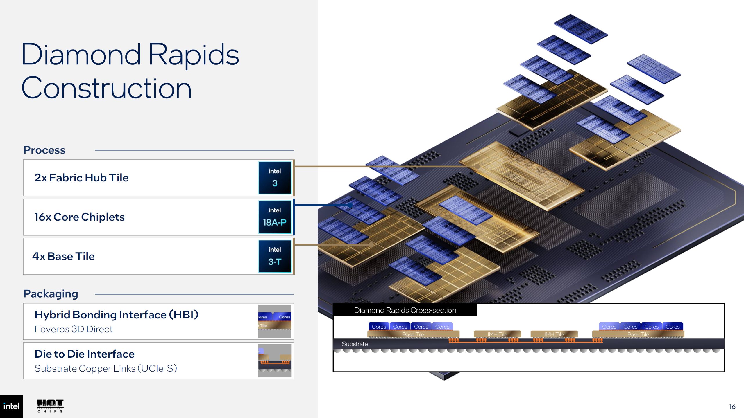
Diamond Rapids将是采用18A-P工艺的首批主力产品之一。据英特尔透露,相关研发工作实际上从上一代Xeon 6+"Clearwater Forest"就已开始,这使得团队能够将E核在性能功耗比方面的优势延续至Diamond Rapids的P核上。Diamond Rapids最高可配置256核心,是上一代核心数量的两倍,因此需要更强的内存带宽支撑。英特尔将IO模块移至封装中心位置,使每个核心都能获得均匀的内存访问延迟,这对AI规模级别的工作负载至关重要,而18A-P带来的频率提升空间也将直接转化为更高的单核性能。
英特尔研究员Eric Fetzer总结道:"这正是你将在Diamond Rapids上看到的效果。一切都从核心底层技术开始。我们借助18A-P的优势同时提升核心数量与核心性能,再通过架构升级为其提供足够的数据供给。"
总体而言,带有背面供电的GAA技术被视为英特尔迈向多代单核性能领先路线图的第一步。这一进程始于18A-P工艺,其在低电压下实现30%的提升,在高电压下实现两位数增幅,且已在量产硅片上得到验证,相关产品包括Diamond Rapids Xeon系列以及计划于明年推出的Nova Lake"Core"系列。
Comments