What is the difference between the chip wafer on board packaging (CoWoP) technology that has been hotly hyped in the market recently and the existing CoWoS packaging? What is the impact on the supply chain? What are the prospects for commercialization? On August 5, according to Zhuifeng Trading Desk, JPMorgan Chase stated in its latest research report that Nvidia is exploring a revolutionary chip packaging technology CoWoP (Chip-on-Wafer-on-PCB), which is expected to replace the existing CoWoS packaging solution.
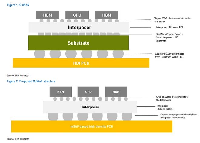
JP Morgan pointed out that this technological change will use advanced high-density PCB (printed circuit board) technology to remove the ABF substrate layer in the CoWoS package and directly connect the interposer layer to the PCB.
The bank also analyzed in detail the impact of "CoWoP" technology on the supply chain in the research report, believing that it is obviously negative news for ABF substrate manufacturers, but it is a major opportunity for PCB manufacturers.
Although analysts at JPMorgan Chase believe that the probability of commercialization of this technology in the medium term is low, mainly due to multiple technical challenges, the bank emphasized in the research report:
Analysis of CoWoP technical principles, advantages and disadvantages
According to the research report, CoWoP represents the Chip-on-Wafer-on-PCB technology path. After completing the chip-to-wafer interposer manufacturing step, the interposer (with the chip on top) is mounted directly to the PCB (also known as the platform PCB) instead of being bound to the ABF substrate as in the CoWoS process.
Potential advantages of this technology include:
However, JPMorgan believes there are key challenges with this technology. Currently only Apple uses mSAP or SLP PCB technology, but its pitch size is larger and the PCB board area is smaller, so scaling this technology to large GPUs with higher current carrying capabilities remains a technical and operational challenge.
Supply chain impact: significant negative impact on IC substrates, major opportunities for PCB manufacturers
JPMorgan Chase stated in the research report that this is obviously negative news for ABF substrate manufacturers, because the added value of the substrate may be significantly reduced or completely eliminated, and more complex and fine-pitch signal routing will be transferred to the RDL layer (intermediate layer), while the high-end PCB layer assumes the intra-package routing step.
JPMorgan Chase believes that for PCB manufacturers, there is a major opportunity at high speed. The research report states:
Therefore, the bank believes that companies with advanced mSAP capabilities and in-depth knowledge of substrate/packaging processes will have an advantage.
The probability of commercialization in the medium term is low, which will not hinder Nvidia’s continued strengthening of its innovation leadership.
JP Morgan analysts believe that due to multiple technical challenges, the probability of commercialization of CoWoP in the medium term is still low.
Historically, higher I/O counts and finer line/space dimensions (down to 5 microns for CoWoS-L and ~10 microns for CoWoS-S) required migration to ABF substrates. For AI accelerators, even ABF substrates are expected to fail after 5/5 line/space dimensions.
Even if PCB technology uses mSAP, it can currently only achieve line/space widths of 20-30 microns, which still leaves a large gap compared with expected performance.
According to previous news from Zhuifeng Trading Desk, Morgan Stanley also stated that the current L/S of high-density interconnect (HDI) PCB is 40/50 microns, and even the substrate-like PCB (SLP) used for iPhone motherboards only reaches 20/35 microns. There are significant technical difficulties in reducing the L/S of PCB from 20/35 microns to below 10/10 microns.
In addition, JPMorgan Chase believes that Nvidia’s currently determined roadmap (developing towards CoWoS-L, CoPoS, using GPU sockets in Cordelia Board) is also quite contradictory to the new direction pursued by CoWoP.
Supply chain research shows that high value-added packaging ecosystem players (such as TSMC) are not highly involved and are mainly concentrated in PCB manufacturers and specific OSAT manufacturers, which reduces the possibility of commercialization.
However, JPMorgan Chase pointed out that regardless of whether CoWoP is successfully mass-produced, Nvidia will continue to lead data center AI infrastructure innovation through a system-level approach.
JPMorgan Chase said that this continuous innovation capability is expected to enable Nvidia to maintain its leading edge in the GPU field in the next few years and occupy a dominant position in the competition with ASICs.