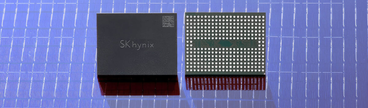
SK Hynix announced today that its 321-layer 2TB QLC NAND flash memory product has completed development and has begun mass production. This move marks the first time in the world that QLC technology has been used to achieve more than 300 layers of NAND flash memory, setting a new benchmark for NAND density. The company plans to officially launch the product in the first half of next year after completing global customer validation.
To maximize the cost competitiveness of the new product, SK hynix developed a 2Tb device with twice the capacity of existing solutions. In order to solve the performance degradation problem that may be caused by large-capacity NAND flash memory, the company increased the number of independent operating units (Planes) in the chip from 4 to 6. This enables greater parallel processing capabilities and significantly improves simultaneous read performance.
As a result, 321-layer QLC NAND not only offers greater capacity but also higher performance than previous QLC products. Data transfer speeds are doubled, write performance is improved by up to 56%, and read performance is improved by 18%. In addition, write power efficiency is improved by more than 23%, enhancing the competitiveness of AI data centers where low power consumption is critical.
The company plans to first apply its 321-layer NAND to PC SSDs before expanding to enterprise SSDs (eSSDs) in data centers and UFS for smartphones. Leveraging its proprietary 32DP3 technology, which can stack 32 NAND chips simultaneously in a single package, SK Hynix aims to tap into the ultra-large-capacity eSSD market for AI servers by achieving twice the integration density.
Jeong Woopyo, head of NAND development at SK Hynix, said: "With the launch of mass production, we have significantly enhanced our high-capacity product portfolio and ensured cost competitiveness. We will make a major leap as a full-stack AI memory supplier to meet the explosive growth of AI demand and the high-performance requirements of the data center market."