Japan is accelerating its return to the top ranks of the semiconductor industry, and Hokkaido has become the center of this renaissance. The island, known for its cow pastures, ski resorts and summer flower fields, is now home to one of the world's most ambitious chip-making projects - the government-backed Rapidus fab. The foundry aims to achieve a breakthrough in mass production of 2nm logic chips.
The significance of this project is extraordinary, both on a political and economic level. Tokyo has committed about $12 billion to Rapidus, which is only part of the "semiconductor subsidy" market. In addition, local giants such as Toyota, SoftBank and Sony have also joined the ranks of support.
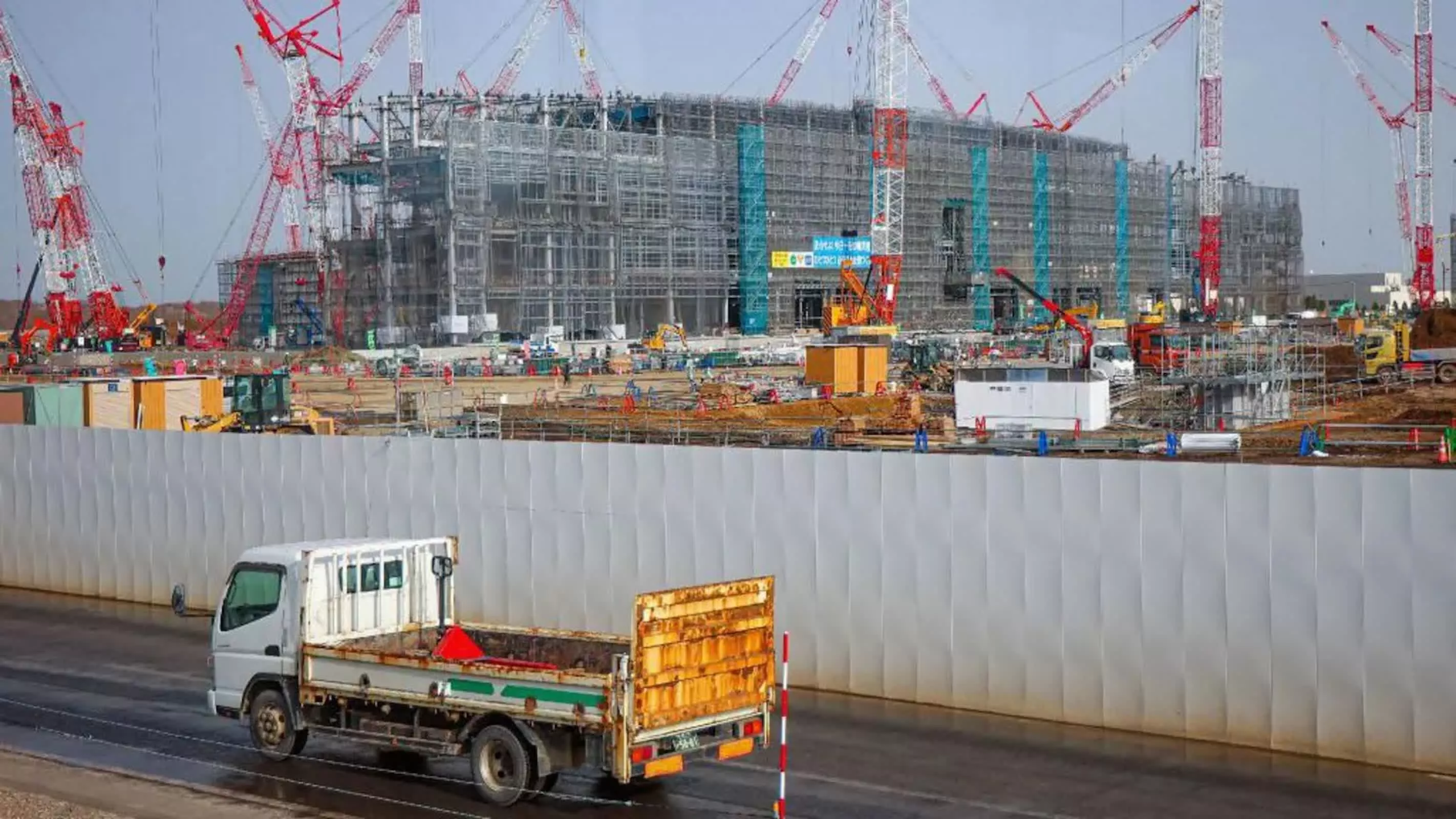
The new factory is called "IIM-1 (Innovative Integrated Manufacturing)" and is located in Chitose City, close to the New Chitose Airport and within commuting distance of Sapporo City. It is located in the Bibi World Industrial Park. The site was chosen for its stable water and electricity supply and lower earthquake risk than other candidates in Japan - crucial for highly sensitive lithography equipment.
The factory design takes into account both industrial and regional characteristics. Rapidus CEO Junyoshi Koike said that the exterior of the factory will be covered with grass and blend in with the pastoral landscape of Hokkaido. Behind this green shell, there is a planned front-end and back-end integrated manufacturing base: the first 2-nanometer trial production line is planned to be put into production first, and large-scale mass production is expected to start in 2027.
From a technical perspective, Rapidus is trying to enter the market at the most demanding stage of the process node. Earlier this year, the company announced that it had successfully trial-produced 2-nanometer gate-all-around (GAA) transistors. This achievement was due to its cooperation with IBM and the introduction of IBM's nanosheet process intellectual property.
Currently, only TSMC and Samsung have demonstrated similar capabilities in this process field, while Intel has adopted a different development route and will jump directly from 7 nanometers to about 1.8 nanometers without setting up a 2-nanometer node transition.
For Japan, the significance of being able to realize usable 2nm devices on 300mm wafers is not to catch up with competitors in the short term, but to prove that local engineers have the world's leading GAA integration capabilities.
Rapidus has installed ASML's latest extreme ultraviolet (EUV) lithography machine at the IIM-1 factory, becoming the first Japanese company to deploy this level of equipment in advanced logic manufacturing. This equipment comes from ASML's high-production line and can process hundreds of wafers per hour at full load. It integrates high-power light sources, precision optical components and ultra-high-speed wafer platforms.
Putting this equipment into use requires a high degree of coordination in factory construction, clean room preparation and equipment delivery, and strictly meets the temperature, humidity and cleanliness specifications required for EUV operation.
On the production side, Rapidus adopts a different process architecture than most mature factories. The company plans to run all front-end processes on single-wafer equipment instead of the commonly used batch/single-wafer hybrid. That is, each wafer independently undergoes deposition, etching, cleaning and other processes, allowing engineers to adjust parameters in real time and collect high-resolution data at each layer.
This data-driven process helps reduce defect density and speed up yield improvement, especially at demanding nodes like 2nm, where even tiny changes in line width, offset or sidewall details may cause chip failure. Rapidus believes that early detection of processing deviations and anomalies can shorten the cycle from tape-out to certified mass production, and build its selling point of "quick response and customized manufacturing" instead of directly competing with large foundries for production capacity.
Rapidus is also simultaneously building a packaging ecosystem. Near Chitose City, Seiko Epson has deployed RCS (back-end pilot production line) in its facilities to develop redistribution layer interposers, die integration and 3D packaging processes. These technologies will transition to the IIM-1 back-end production line in 2027, enabling them to realize an integrated industrial chain from transistor manufacturing to advanced packaging and testing, forming a "high-quality known good product" assembly system to improve yield rates.
Despite the political momentum, there are still doubts about its structural obstacles. The ASEAN+3 Macroeconomic Research Office estimates that Rapidus still has a large gap in its current funding of about 5 trillion yen (approximately US$31.8 billion) required to achieve large-scale mass production of 2 nanometers. Analysts from the Center for Strategic and International Studies also pointed out that Rapidus has no actual achievements in the field of advanced manufacturing and relies heavily on the technology transferred by IBM, which is far less than the deep process accumulation accumulated by TSMC and Samsung over the years.
Therefore, the outcome of Rapidus's transformation battle is full of uncertainty: it must not only put the first batch of new factories in the industry into production smoothly, but also need to transfer the complex process recipes developed overseas locally, reach a commercial level of 2nm yield, attract stable customers, and verify that its "single wafer + AI intelligence" production model can really shorten the production cycle.
If most of these goals can be implemented, Japan will regain its position at the forefront of semiconductor manufacturing. If it fails, IIM-1 may become a typical case of "wanting the king to return but being defeated by reality."