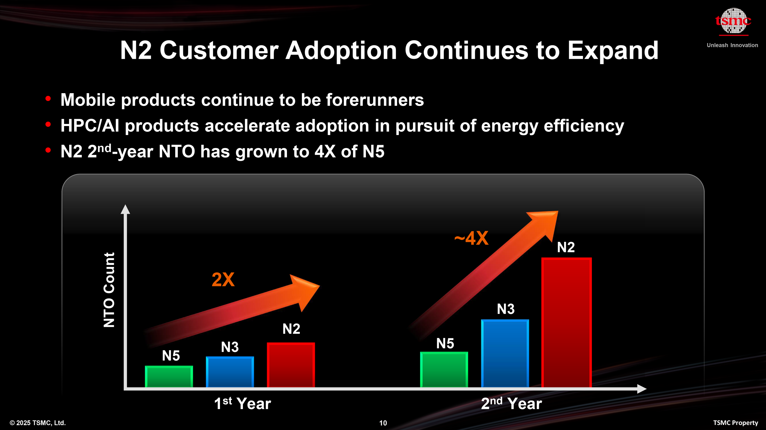
TSMC has started large-scale mass production of the N2 2nm process, but it is very low-key and there is no official announcement, but it is completely consistent with the previously formulated progress plan. The 2nm process professional questions page on TSMC’s official website has this sentence:"TSMC's 2nm technology has been put into mass production in the fourth quarter of 2025 as planned."
Next year, TSMC's N2 production capacity will ramp up rapidly to accommodate various products, including NVIDIA, AMD, Apple, Qualcomm, and MediaTek.

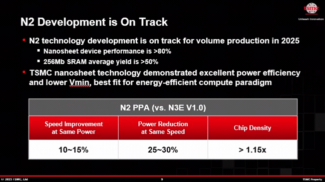
N2 is TSMC’s first process node to apply GAA (gate-around nanosheet transistor), which is somewhat similar to Intel RibbonFET.
This technology completely wraps the conductive channel composed of horizontally stacked nanosheets through the gate, optimizing the electrostatic control effect and reducing the leakage rate, thereby further reducing the size of the transistor and increasing the density without sacrificing performance and energy efficiency.
The N2 process also integrates ultra-high performance metal-insulator-metal capacitors (SHPMIM) in the power supply part.,电容密度比之前的高性能金属-绝缘体-金属电容器(SHDMIM)提升超过2倍,同时将薄层电阻(Rs)、通孔电阻(Rc)降低了50%,从而提升供电稳定性、芯片性能、综合能效。
按照台积电给出的说法,N2相比N3E同等功耗下性能提升10-15%,同等性能下功耗降低20-25%,晶体管密度则提升15%。
There are two subsequent upgraded versions of the N2 process.N2P expects mass production in the second half of 2026, the performance will be improved by another 5-10%, and the power consumption will be reduced by another 5-10%.
N2X will be mass-produced in 2027, compared with N2P, the performance continues to be improved by 10%, and the power consumption is further reduced.
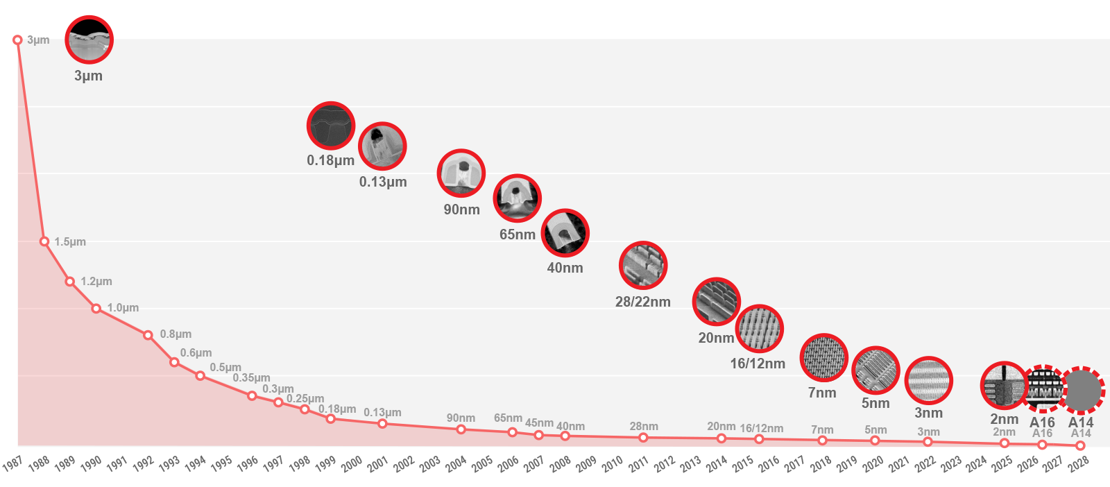
After that are A16 and A14. The former has the industry's first super power supply circuit (SPR), and mass production will be promoted as scheduled in the second half of 2026.