Recently, Tesla Korea released a recruitment message for AI Chip Design Engineer, indicating that Tesla’s self-developed chip plan has entered an accelerated stage. Elon Musk also said on the social platform
This wave of layout focuses on mass production preparations for the next generation of AI5 and AI6 chips. Tesla adopts a factory-based R&D model and conducts in-depth technical cooperation with Samsung and TSMC to improve the yield and performance of high-end processes. With the development of Robotaxi and Optimus, the demand for computing power continues to rise, and the ability to self-research chips has become a key support.
Tesla Korea’s recruitment reveals first-principles talent outlook
Tesla’s recruitment method this time continues Elon Musk’s consistent style. Applicants do not need to submit a lengthy resume, but directly state "the three most difficult technical problems they have solved" and send it to the official mailbox. This screening mechanism emphasizes practical experience and problem-solving abilities rather than pure academic background, which helps identify engineering talents with practical experience in mass production.
Choosing to recruit chip designers in South Korea also has strategic considerations. South Korea not only has advanced process production capacity such as Samsung, but is also a center for HBM (High Bandwidth Memory) technology, including SK Hynix and Samsung as core suppliers.
With AI5 and AI6 facing FSD, the large amount of imaging and neural network calculations required for unsupervised self-driving will inevitably rely on high-bandwidth storage support. Tesla has established a local team to participate in the prototype verification process of Samsung's Hwaseong factory nearby, and conduct software and hardware co-design (Co-design) with the storage supply chain to shorten the gap between design and mass production.
Differences in foundry strategies and specifications of AI4, AI5 and AI6
As Tesla's self-developed chip blueprint gradually becomes clear, its supply chain structure also becomes clearer, forming a dual-foundry layout. Through division of labor and cooperation with different foundry partners, Tesla retains greater flexibility in process nodes and production capacity allocation to reduce single-source risks.
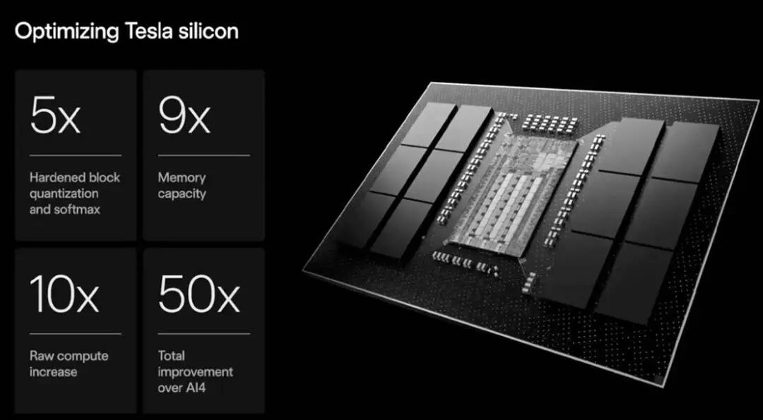
Tesla AI chip performance improvement: Compared with AI4, the hardened block quantization and softmax functions are increased by 5 times, the storage capacity is increased by 9 times, the raw computing power is increased by 10 times, and the overall performance is increased by 50 times.
AI5 and AI6 will correspond to the HW5 and HW6 platforms respectively and become the computing core of the new generation of vehicle systems. Among them, AI5 supports transitional products and advanced driving assistance functions, while AI6 targets fully autonomous driving scenarios and provides basic computing power for future Robotaxi and higher-end FSD applications.
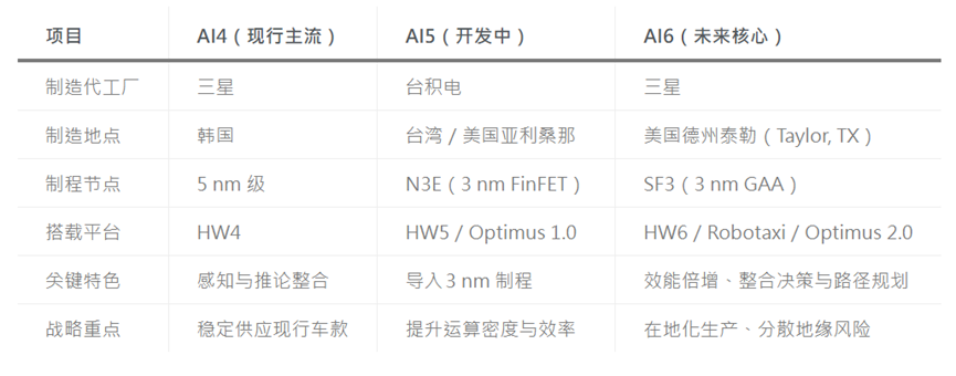
Tesla’s self-developed AI chip specifications and production layout
Why did AI6 switch to Samsung's Tyler, Texas plant?
Although TSMC has a mature advantage in the 3nm process, Elon Musk decided to hand over the main production capacity of AI6 to Samsung's Tyler, Texas plant. The considerations behind this include supply chain risks, policy incentives and cost structures.
First of all, in terms of production capacity allocation, Tesla uses a dual-factory model to diversify risks and avoid over-reliance on production in a single region. This move will help reduce the impact of geopolitical or regional emergencies on chip supply and improve long-term supply stability.
Secondly, Samsung’s Tyler, Texas, factory meets the subsidy conditions of the U.S. Chip and Science Act (CHIPS Act) and is close to Tesla’s Texas headquarters. The design team and production line engineers can collaborate nearby to shorten the time from design, verification to mass production introduction.
In terms of business conditions, Samsung provides competitive OEM quotations and technical support solutions in order to secure an 8-year cooperation agreement worth approximately US$16.5 billion. This allows AI6 to strike a balance between cost and production capacity guarantee, and also increases Tesla’s bargaining space in the advanced process generation.
The significance of AI6 for unsupervised self-driving and humanoid robots
AI6 is positioned not only as a generational upgrade of on-board computers, but also as the core foundation for Tesla’s advancement of Embodied AI. When computing requirements expand from assisted driving to autonomous driving and humanoid robots, the chip architecture will inevitably be reconstructed simultaneously.
In terms of architectural design, AI6 is expected to integrate functions such as perception, decision-making, and image processing that originally required the cooperation of multiple chips into a single SoC to form a more integrated computing platform. This can reduce power consumption and data transmission latency, and improve system stability.
In terms of production capacity planning, if Optimus enters the stage of large-scale mass production, each robot will need to be equipped with a high-performance AI6 chip, and the overall demand scale will be much higher than the current automotive market.
In addition, in order to meet the needs of high bandwidth and high computing power, AI6 is expected to introduce advanced packaging technologies, such as TSMC CoWoS or Samsung I-Cube and other heterogeneous integration solutions, to improve data exchange efficiency and support real-time inference of large neural network models.
Opportunities and challenges in Taiwan’s semiconductor supply chain
In the short term, TSMC still holds the main orders for AI5, and Tesla Dojo chips continue to use TSMC’s advanced packaging InFO-SoW. However, as Tesla expands its R&D layout in South Korea and promotes the localization of some advanced processes in the United States, the division of labor in the global supply chain is undergoing adjustments.
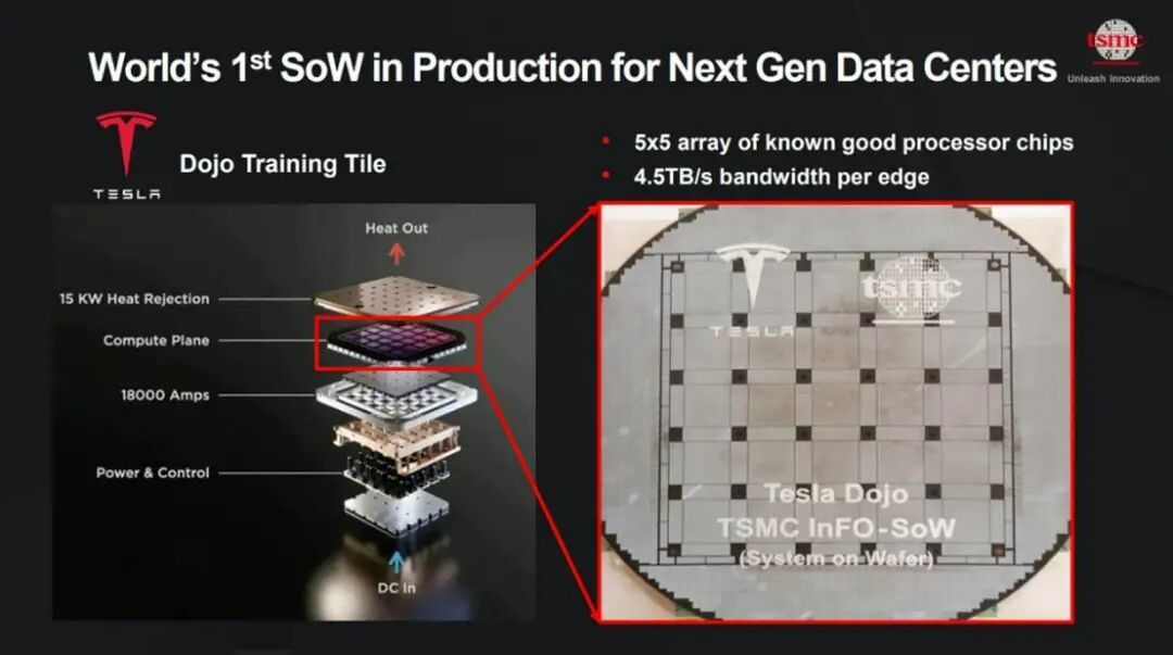
Tesla Dojo training chip: the world's first mass-produced System on Wafer (SoW) AI processor, using TSMC InFO technology, a 5×5 known good chip array, a bandwidth of 4.5 TB/s per side, and supports 15 kW heat dissipation and 18,000 A current input.
For Taiwan's supply chain, the key lies not only in advanced process capabilities, but also in the leadership of back-end integration technologies, including chiplet (small chip) integration, silicon photonics technology, and higher-end packaging and testing capabilities. If the technology gap can be maintained in the fields of heterogeneous integration and high-speed interconnection, it will help consolidate its core position in the AI chip era.