TSMC captured 70% of the global wafer foundry market last year, and its advanced technology can be said to be far ahead of other competitors. The latest process for mass production is 2nm, but the 1nm process is also on the way. The park land that needs to be prepared first before 1nm builds its factory. It was recently reported that the Sharon Park in Tainan, with a total area of 531 hectares, will enter the second phase of environmental impact assessment in April this year, and the final environmental impact assessment will be completed in the third quarter of 2027.
After that, it can be handed over to TSMC to build a factory. The initial scale is expected to be at least 200 hectares.
According to TSMC’s previously announced plan, six wafer fabs will be built in the Sharon Park, among which P1 to P3 are mainly for the 1.4nm process A14.The P4 to P6 factories are oriented to the 1nm process, and it is not ruled out that there will be a 0.7nm process in the future.
In the roadmap currently announced by TSMC, the N2 process of the 2nm process was mass-produced at the end of last year. This year it will be commercialized on a large scale by Apple, AMD and other companies. The A16 process is the first launch of NVIDIA's Feynman GPU. It will be trial-produced at the end of this year, and mass production will not be until 2027.
After A16 is the A14 process, which is the 1.4nm level. It will upgrade the second-generation GAA transistor structure and back power supply and is expected to be released in 2028.
Next up is the 1nm process we are talking about now, but TSMC has not released much information before.By convention the naming will be A10, this is also TSMC's first angstrom-level process - the title of the world's first has been occupied by Intel's 20A process a few years ago, but the latter is a bit unworthy of its name. It has not achieved the honor of the angstrom process before reaching below 1nm.
However, the technical details of TSMC's 1nm process are still unknown. It is rumored that the transistor structure will be further upgraded from GAA to CFET, and it is even said that 2D materials will be used. It is difficult to judge what will happen in the end.
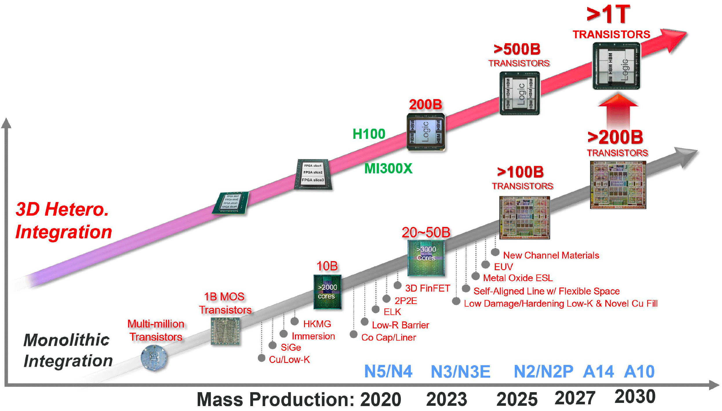
The 1nm process is expected to be launched in 2030 according to TSMC's node. One of the goals they proposed in 2023 is to integrate 200 billion transistors on a single chip at the 1nm node.3D packaging reaches 1 trillion transistors,This goal is the same as Intel's previous call for 1 trillion transistors. It depends on who can achieve it first.