Musk announced the largest chip manufacturing plan in history. On March 22, local time, Tesla CEO Elon Musk disclosed on the
The project will serve electric vehicles, humanoid robots and space AI infrastructure, and is regarded as a key measure for Musk to break through the bottleneck of global chip supply. Musk made it clear that Terafab will be an integrated facility with two fabs, each focusing on one chip design to maximize manufacturing efficiency and iteration speed.
On the evening of the 21st local time, he officially announced the launch of the Terafab plan for the first time at a public event in Austin.
According to the plan, the two fabs have a clear division of labor: one is used to produce edge inference chips to support Tesla's autonomous driving system and Optimus humanoid robot; the other focuses on space-specific radiation-resistant high-performance chips and is deployed in SpaceX's orbital AI data center network. Musk emphasized that space chips need to adapt to extreme temperatures and radiation environments, and solar-powered orbital data centers are expected to surpass ground facilities in terms of energy efficiency and cost.
"Either Terafab is built, or we will have no chips available," Musk said bluntly in his speech last Saturday. He said that the current global chip production capacity can only meet a small part of his company's future needs; although TSMC, Samsung, etc. are still key suppliers, their production expansion speed cannot match the growth rate of computing power demand of Tesla, SpaceX and xAI, which has become the core motivation for him to promote the "self-research + self-manufacturing" strategy.
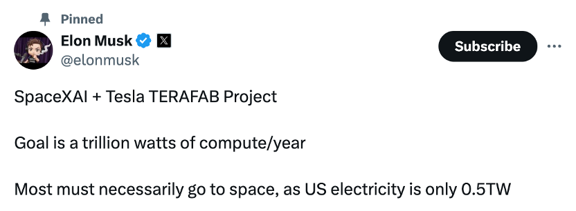
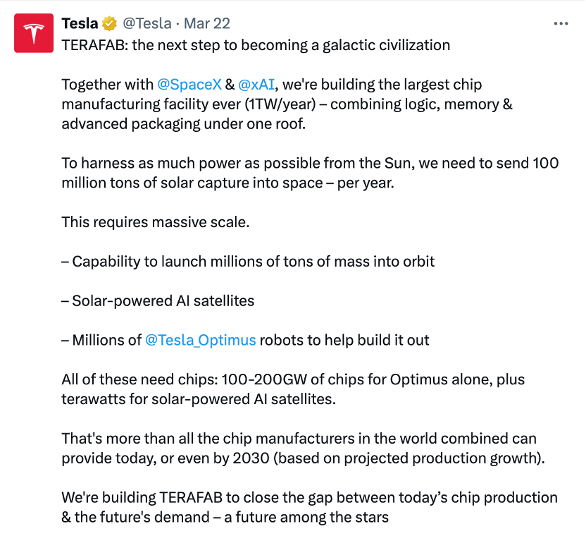
According to Musk's description, Terafab's long-term goal is extremely ambitious: an annual computing power production capacity of 1 terawatt (TW), which is equivalent to about 50 times the current total annual computing power of AI chips in the world. Musk also pointed out that the annual power generation in the United States is about 0.5 TW, highlighting the energy constraints of ground computing power expansion, so it plans to invest 80% of its production capacity in space orbital AI infrastructure, and only 20% for ground applications.
Tesla issued a document stating that Terafab is "the largest chip manufacturing factory in history" and integrates the entire process of logic chips, memory chips and advanced packaging in the same factory. In order to maximize the use of solar energy, 100 million tons of solar energy capture equipment need to be transported to space every year.
According to Bloomberg, SpaceX is preparing for an IPO with a target valuation of over US$1.75 trillion; the company has completed the all-stock acquisition of xAI in February 2026 to strengthen the collaboration between AI and space data infrastructure. In this context, Terafab is not only a manufacturing project, but also an underlying computing hub connecting electric vehicles, AI and aerospace businesses.
In recent years, Tesla has continued to increase investment in self-developed AI chips, SpaceX has accelerated the construction of a global satellite network, and xAI has rapidly expanded its large model training computing power. The combination of the three has caused exponential growth in chip demand.
However, market analysts believe that there are still major uncertainties in project advancement: Musk has not disclosed specific construction schedules and mass production nodes; advanced semiconductor manufacturing is a highly technology- and capital-intensive industry, and industry estimates indicate that the Terafab project is expected to have a total investment of US$20 to 25 billion; some of Musk's past high-risk projects have been delayed, and the market is cautious about its execution capabilities.